


Optimizing Optoisolators, and Other Stories of Making Do With Less
It’s been a few months since I’ve rolled up my sleeves here and dug into some good old circuit design issues. I started out with circuit design articles, and I’ve missed it.
Today’s topic will be showing you some tricks for how to get more performance out of an optoisolator. These devices — and I’m tempted to be lazy and call them “optos”, but that sounds more like a cereal with Greek yogurt-covered raisins — are essentially just an LED and a phototransistor inside an opaque package. On one side of the package, you put in current through the LED. It lights up. You don’t see it because the light is inside the package, and it’s designed to shine onto the phototransistor and turn it on. (If the package weren’t opaque and you could see the LED light up, that would also mean that you could shine light from outside onto the phototransistor and turn it on, which is not good, because the only time you want the phototransistor to turn on is when the LED turns on. If you’ve ever used the old transparent glass-packaged 1N914 / 1N4148 diodes and found that your circuit output changes when the fluorescent lights are on, you’ll be thankful optoisolator packaging is opaque.) Current goes in on one side, this causes current to flow on the other side, and there is no galvanic connection between input and output, so you can send a signal across a high-voltage differential. Most optoisolators have an input-output rating anywhere between 500V and 5000V.
The easiest way to work with optoisolators is to buy the kind that has built-in input and output signal conditioning, and that way, you can pretend that they’re not optoisolators, and just treat them like a black box. Logic signal in, logic signal out, galvanic isolation in between. In fact, if I want to send a high-speed digital signal across a voltage isolation barrier, I would probably not use optoisolators, but instead something like the Si8715 or Si8620BB or ISO7220C, which are actually based on capacitive coupling, rather than optoelectronics. The capacitive-coupling digital isolators are supposed to be more reliable, and don’t show signs of temperature dependence and aging that are seen in optoisolators.
The problem is price. A quick glance at Digi-Key shows the Si8715 (single-channel 15Mbps) shows up at around $1.07 at 1000-piece quantity, the ISO7220C (dual-channel 25Mbps) at $1.18, and the Si8620BB (dual-channel 150Mbps) at $1.26, with prices going up from there. Whereas the cheapest optoisolators are the LTV-817 and EL-817 at just under 10 cents each in 1000-piece quantity.
So when you’re working on a high-volume product, where pennies matter, and the accountants and managers come knocking at your door, you may not get to use those nice easy black-box ICs.
On the other hand, the LTV-817 and EL-817 are jellybean optoisolators — they are SLOW, and you may find it difficult to get even 50Kbps out of them.
The next best level of niceness, below the fancy black-box digital isolator, is the 6N137. This is a quasi-digital optoisolator with “logic output”, sold by almost every manufacturer in the optoelectronics business — essentially, it has an LED input that shines through an electrostatic shield onto a photodiode connected to a comparator with open-collector output. It’s relatively fast, supporting a guaranteed 10Mbps. Oh, and you get an output enable pin for free.
The cheapest 6N137’s are made by Lite-On and Everlight — the same Far East makers of the LTV-817 and EL-817; big surprise there — and ring in at just under 25 cents in 1000-piece quantities. And if that price makes the bean-counters happy, you’re golden. (For some reason, the dual version of this, the HCPL-2630, doesn’t seem to come in a cheap version; Everlight allegedly sells an EL2630, but none of the distributors seem to carry it, and the datasheet they list is the wrong one, for the 6N137 instead.)
If 25 cents is too much, but the 10 cent parts are too slow, you’ve got a hodgepodge of other optoisolators in between. I’ll show you my recommendation of what to do in this price range in a minute.
But first I need to go on a short tangent and vent.
WTF Is Going Wrong
The year was 1998. I had been working about 18 months after graduating college. The year before, I was assigned responsibility for a battery charger in a medical device, and I designed and built some prototype chargers around some power supply modules from Vicor. They worked well, but were too expensive to go into production. We had started working with a contract manufacturer to help us redesign parts of our system, and reduce cost and increase manufacturability. And I worked with a fellow named… well, let’s just call him William Tango Foxtrot. We had kind of an odd battery pack, and the charger needed a custom design. It was Mr. Foxtrot who came up with that design, to meet the specification I wrote.
In retrospect, I should have run away when I realized Mr. Foxtrot was a sub-sub-sub-sub-contractor. My employer was a design house for medical devices; we had design responsibility of a product for a major medical device company which didn’t do their own engineering. My company did have a lot of expertise in medical design, but not high-volume manufacturing, so we worked with the contract manufacturer. And they didn’t do much in the way of batteries, but they did do some business with another company that manufactured battery packs and battery chargers. And this company didn’t do their own battery charger designs; instead, they relied on Mr. Foxtrot. And lucky me, all of us were in different states. So that’s a fourth-level sub-contractor. Or is it fifth? I’m not quite sure how the counting works. And everyone in the chain gets a share of the profits. Anyway, I was barely out of school, so who was I to object?
Several months into this process, Mr. Foxtrot sent us the first few prototypes. They came in a housing designed by the third-level sub-contractor; it was powder-coat black and looked vaguely like Darth Vader’s mask. These prototypes had issues. For one, we’d been using the SMBus as a smart battery communications bus. The battery requests a certain amount of current, and the charger is supposed to deliver up to that current. Pretty straightforward. So Mr. Foxtrot used a PIC16C72 microcontroller to handle the communications. But this charger caused enough electromagnetic interference that it disrupted the communications, and it stopped and displayed a fault. And some of the circuit boards had some problems....
Mr. Foxtrot’s design at this point was like a rotten onion. On the outside it looked kind of okay, but maybe smelled a little odd, and when we pulled off one layer of the onion, we could see the rot, but then when we pulled off a few more layers it was okay. Except the smell didn’t go away. So we pulled off another layer, and there was some more rot, and then we pulled off a few more layers and it was okay again. But the smell persisted… Here’s what the rot looked like in our case:
We never saw the first round of prototypes Mr. Foxtrot designed. They never made it out of his workshop — he couldn’t get the SMBus communications working at all. We talked a bit, and found out he was using a two-layer circuit board, which is a little bit sketchy when you are working on a switched-mode power supply; it makes proper management of electromagnetic noise either difficult or impossible. His original circuit had used some LM324 op-amps as comparators for a PWM generator. We didn’t like that: you shouldn’t use op-amps as comparators. They’re not designed for it. Op-amps are optimized to be nice and linear. Comparators are optimized to be fast. Both are tested to be the way they’re designed. If you use an op-amp as a comparator, when the output goes high or low, and the inputs stray apart from each other, the op-amp saturates, and it may take a long time to come out of saturation. The saturation recovery time of an op-amp isn’t usually specified in the datasheet, and there’s nothing to prevent it from taking milliseconds to recover from saturation. (Milliseconds! Think about that for a bit.) Even if Mr. Foxtrot’s circuit had used a comparator, it was still an ugly circuit; the home-made sawtooth generator, while it functioned adequately, was prone to component variation, and we didn’t trust its ability as a robust PWM generator. So we got him to switch to a four-layer board, and he changed his design to use a TL594 power supply IC.
The second round of prototypes were better, and he sent a few of them to us. I needed to do some tests, so I opened up the cover and looked inside. On the bottom of the circuit board, there were some 18 AWG jumper wires. We called him up and asked about these. He said some of the connections on the circuit board had been open-circuited. Another technician and I looked closer, and we found that the thermal reliefs on some of the vias were the culprit. These each had four spokes, and they were very narrow, so they turned into fuses. We got him to fix the vias and size the thermals properly.
I don’t remember exactly what happened next — maybe one of the pads peeled off, or maybe I measured a trace resistance that seemed to be a bit high — but there was something suspicious about the circuit board; after another call to Mr. Foxtrot, we eventually found out that he had used 1/2-ounce copper. The thickness of the copper plating in a printed circuit board is conventionally measured in ounces of copper used per square foot of board area: one ounce copper, the most common thickness, is 34.8μm. Some boards use thicker copper plating to handle high currents. It’s not uncommon to see 2 oz. copper used in a power supply. I worked on one project where we used 6 oz. copper to carry currents in the 100A range. So when we found out this board used 1/2-ounce copper, we weren’t pleased. It was a cost-cutting measure on a circuit board that needed to handle the current. So he changed it to one ounce copper.
Eventually we got an updated prototype. Meanwhile he was working on the PIC16C72 firmware, and I was checking to see if the hardware design was OK. It still had some problems, which I finally traced down to a ferrite drum-core inductor. These kind of inductors have the magnetic field spilling out the ends of the drum, which not only caused EMI, but also caused flux to couple into the ground plane, essentially creating an extra parasitic winding that was shorted. (Changing flux induced a circulating current in the ground plane, that caused extra power losses.) As a result, excess current flowed in the inductor, and it went into saturation and overheated. So we needed to help cool it down, and add a shield, and I don’t think I was ever able to get that to work.
I’m probably omitting at least five other details I can’t remember on the hardware. On the firmware side, we were getting concerned, as a deadline was approaching and we still had problems. We asked Mr. Foxtrot to give us some information about how the code worked. He didn’t really have any documentation, and it didn’t handle the communications the way we were expecting. So I wrote out some flowcharts of how I wanted the program to behave at a high level, and said make it work like this. And the deadline was getting closer… so we asked to look at the code itself. It turned out he was using an assembler called Parallax SPASM. This used different instructions and made the PIC look more like an 8051 processor to the programmer. Let that sink in — it was an assembler used to program the PIC16 architecture with completely different instructions. Oh, and Mr. Foxtrot wasn’t able to help us for most of the week prior to our deadline; he had a trade show he needed to attend....
At this point we got Mr. Foxtrot out of the picture, and I took over the software design as well, learning SPASM because it was too difficult to convert the code to the native Microchip assembly instructions without the risk of introducing new errors. I got a passable battery charger working in time. That was the only time I have ever worked more than 70 hours in a week, and I don’t plan on doing it again.
In the end, I think that project had two or three subsequent versions of a battery charger design, one where we went back to using Vicor power supplies, and later on someone with more experience did a decent job at making a custom charger that was reasonably-priced.
The moral of this story… well, there are several lessons here.
One is don’t work with subcontractors you can’t trust, and figure out early on whether you can trust them.
The second lesson is to make use of pre-existing economies of scale. I mentioned we had an odd battery pack — the voltage was higher than the usual 6 / 12 / 24V batteries common in other products. If we had used a 24V battery pack, it’s likely we could have just purchased an off-the-shelf charger. But we didn’t, and as a result it raised project risk and engineering costs.
The third lesson is to get your priorities straight. Designs have to work first, and be inexpensive second. If you can get it to work but it costs more than you planned, at least you have a shot at success and can reduce cost in the future. If you can get it cheap but it doesn’t work, then there’s no point.
And finally, if you’re doing something new, it’s foolhardy to plan on reaching an optimal low-cost solution from the beginning. There’s no point. Sure, it’s good to aim towards a reasonable price, just don’t try to get all the cost out from the beginning. The large manufacturers like Apple and Samsung and Dell are able to get cycle times down to the point where they can churn out a new product quickly and have it cheap enough to make a profit at high volumes. But that’s because they have experience doing so, and they have a pipeline of research that feeds into their development process to make sure that low-cost components and subsystems are available. If you’re planning a new product that’s going to take a year or two to ramp up production, the time to optimize a battery charger is not at the beginning, where it’s important to get prototypes out there and learn from them. Even in moderate volume, if there are 5000 units produced and you spend $5 more for a suboptimal battery charger, but you save $40,000 in engineering development costs (vs. the $25000 more it costs for the charger), you’re still ahead of the game. Save your cost-down energy to be ready in time for the volumes in which it will pay off.
So that’s my cautionary tale for today. Despite this, I do strongly encourage you to explore low cost design techniques to make better use of the components you have available. Get some experience with these techniques, so you’re ready when you need them. (We’ll talk about a few of these techniques shortly.) Just make sure you have a good idea when you should use them, and when you shouldn’t.
Back to Optoisolators, and the Fading Art of Bipolar Transistor Circuit Design
We’ll get back to the optoisolators in a moment. One more quick comment before we do, though:
Three or four decades ago, if you mentioned transistors, the implication was that you were probably talking about bipolar transistors rather than MOSFETs. NPN, PNP, base, collector, emitter. Collector current equals base current times beta. Early effect. VBE. Blah blah blah. Yep, bipolar transistors. And good designers knew how to make use of them. The fastest computers used bipolar transistors in emitter-coupled logic (ECL), and even the more garden-variety logic chips that had decent performance were 7400 S or AS with Schottky-clamped diodes. Power bipolar transistors might have a current gain in the 8-10 range, and there were all sorts of tricks for driving them on and off quickly.
Nowadays the semiconductor industry has overwhelmingly switched to CMOS, not only for digital logic and microprocessors, but also for analog and power semiconductors, primarily because of its low static power utilization. Optoisolators are one major exception: the devices in optoelectronics are still primarily bipolar phototransistors.
Although bipolar transistors will probably be around for a while, I think the techniques of using them are at risk of becoming obscure. And every so often, they find a niche usage in your circuits. So you’ll want to at least understand a few things about NPN and PNP transistors, and know where to look to find out more.
The essential difference between a bipolar transistor and a MOSFET, from a circuit design standpoint, is that bipolar transistors are current-driven devices and MOSFETs are voltage-driven devices. In both, the primary current (collector-emitter in bipolars, drain-source in MOSFETs) is relatively independent of the voltage across the device, and strongly dependent on what’s going on in the control terminal: in its linear range, bipolar transistor emitter-collector current is proportional to base current, whereas MOSFET drain-source current is a somewhat nonlinear function of gate-source voltage. That’s the static behavior.
The dynamic behavior of both bipolar transistors and MOSFETs is more interesting and perhaps less well-known. I know of three factors that influence switching time in bipolar transistors (two of them also apply to MOSFETs):
-
Base-emitter capacitance. (similar in MOSFETs) One of major factors that influences the effective bandwidth of a transistor is capacitance seen at its input terminal. This capacitance has to be charged up to turn the transistor on, and discharged to turn it off.
-
Base-collector capacitance, aka the Miller effect (similar in MOSFETs). The voltage gain between base and collector causes an effective multiplication of capacitance seen at the base. This means that a lower voltage gain, due to a lower load impedance at the collector, will raise the bandwidth of the transistor.
-
Base-collector saturation. When the transistor collector-to-emitter voltage drops to the point where the base-collector junction becomes forward-biased, this stores additional charge. Turning off a transistor in the saturation region requires extra charge to be removed.
Good transistor drive circuits keep all three of these effects in mind, using essentially the following techniques:
-
Push charge in, pull charge out during switching. (We do this as a matter of course in MOSFETs.)
-
Keep collector impedance low, reduce magnitude of switching.
-
Keep base-collector junction from saturating. (Circuit designers typically use a Schottky diode clamp or a technique called the Baker clamp to keep the collector in an NPN transistor just above the saturation voltage.)
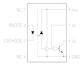
So let’s look at our optoisolator again. The LTV-817 and EL-817 are four-terminal devices: cathode and anode of the input photodiode, and collector and emitter of the output phototransistor. The exposure of light onto the phototransistor essentially acts in place of the normal base current.

We don’t have access to the base, so the only technique available here is the second in our list: keep the output impedance low. In fact, if we look at the LTV-817 datasheet, we can see this graph:
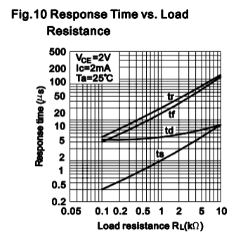
Response times are much faster with a lower output impedance. So if you want high speed, don’t skimp on output current.
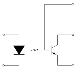
The other techniques would be available to us if we had access to the base terminal. It turns out that there actually are optoisolators which give us access to the base terminal. The 4N35/4N36/4N37 are standard parts made by many manufacturers, and they aren’t very expensive. Digi-Key carries one from Lite-On for 11.3 cents in 1000-piece quantities, not much more than the LTV-817. Here’s what we get:
The third technique listed above, keeping the base-collector junction from saturating, is possible to use, if we connect a Schottky diode from base to collector; this keeps the collector from going more than about 0.3V below the base. This will speed-up turn-off times. Digi-Key shows some of the BAT54 Schottky diodes at 3 cents apiece in 1000-piece quantities.
The first technique listed above, pushing charge in or pulling charge out, is possible to use as well. In a plain transistor circuit (as opposed to a phototransistor), the base current would come from a voltage through a resistor, and we could add parallel capacitance to this resistor. We can’t do this directly with a phototransistor, since the source of the base current comes from light from the LED. We could put a capacitor in parallel with whatever resistance we use to drive the LED, and it will add a short high-current pulse when the LED is first turned on. This should allow the phototransistor to be turned on faster. This capacitor isn’t going to help us turn the phototransistor off faster, however: we can’t use the LED to pull photons out of the phototransistor to get a negative base current. But we can help it turn off faster, by connecting a resistor between base and emitter. This is done with plain transistor circuits as well: it helps pull current out of the base, which speeds up the turnoff time. (Without that resistor, the only way for charge to get pulled out of the base is via the base-emitter current, and it takes a while to decay.)
This is a useful technique, and I don’t understand why optoisolator manufacturers don’t suggest doing this in their datasheets. The idea is that you figure out the minimum amount of equivalent base current caused by light falling onto the phototransistor, and budget some of it towards flowing through the base-emitter resistor. Unfortunately most manufacturers don’t spec the beta (aka hFE) values of their transistors, so it’s not possible to guarantee through specifications. (One exception: TI’s 4N35 lists a typical hFE of 500.) But if you’re willing to do some experiments and leave plenty of margin, you should be able to get some speedup with a small base-emitter load. Something in the 100kΩ range (robbing about 6μA of base-emitter current while the phototransistor is on) is about right. The Fairchild datasheet for the 4N35 series actually gives some useful characterization graphs involving base-emitter resistance; for example:
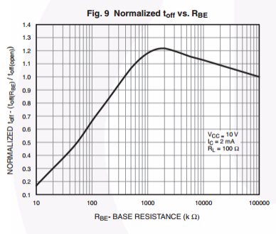
Here, if RBE is present, but it’s a very high value (1-100MΩ), the off-time actually increases. I’m not really sure why that is, but the important point is that as the resistance goes down, the off-time decreases. My rule of thumb would be to see how low of a resistance you can go without preventing the transistor from turning on, and then multiply that resistance by something in the 5-10 range so you have plenty of margin.
So here’s our adjusted circuit:
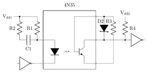
R1 and R4 are the basic resistors setting input current and output load. The 4N35 is optimized for 100% current transfer ratio (CTR) at 10mA input current. With a 3.3V ± 5% supply, to get at least 10mA, I would set R1 around 150Ω since the input LED can drop up to 1.5V, and the driving gate on the input probably won’t pull down all the way to 0. Then the output load resistance R4 should be 330Ω to make sure the output signal swing is large enough to guarantee a valid logic low input to downstream circuitry.
Speedup capacitor and resistor C1 and R2 may be difficult to use without drawing too much current, so if I were creating a circuit board, I would keep them in my design as an insurance policy, but I would probably leave them unpopulated.
Schottky clamp D2 is a BAT54 diode, which serves to keep the phototransistor from entering saturation. For base-emitter resistor R3 we’ll try using 100KΩ.
If I wanted to speed things up a little more, I’d reduce the output swing of the phototransistor and use another inversion stage:
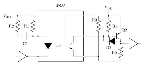
Here we can set R4 to 100Ω — for 10mA output current, we’ll get 1.0V swing, enough to guarantee that PNP transistor Q2 turns on; we can set its load resistor R5 to something that’s a compromise between sinking too much current and keeping load resistance low: 470Ω is probably about right. A 2N3906 equivalent is fine for Q2. (Digikey lists NXP’s PMBT3906 as being just over 2 cents each in 1000 piece quantities.) Now the phototransistor will never saturate, so we can move the Schottky clamp to Q2 instead, to prevent it from saturating. Or maybe we can just get rid of the Schottky clamp — standalone switching transistors like the 2N3906 are generally faster than phototransistors, so the time for Q2 to come out of saturation probably won’t be too much, especially since there’s a 100Ω resistor from its base to emitter, to help it turn off quickly.
Anyway, hopefully you’ve gotten some ideas for how to treat your transistors like the thoroughbreds they are, and let them come closer to achieving their maximum potential. To sum up, I’ll restate the three factors to keep in mind when you want to keep bipolar transistors switching quickly.
-
Base-emitter capacitance. Push charge in, pull charge out during switching, and/or keep base-emitter resistance as low as practical.
-
Base-collector capacitance. Keep the collector impedance low, and/or reduce the magnitude of the voltage swing.
-
Base-collector saturation. Keep the base-collector junction from saturating. One way is to reduce the magnitude of the voltage swing, so there is always at least a volt or two between collector and emitter, and the other is to use a Schottky clamp or Baker clamp to keep the collector in an NPN transistor just above the saturation voltage.
Please note: if you use solderless breadboards like the one below (thanks again, Wikipedia!), there are a few pF of parasitic capacitance between adjacent rows, and you will get slightly worse performance than if you used a perfboard or custom circuit board. One trick to reduce this impact on critical circuit nodes used in solderless breadboards, is to leave an empty row between each circuit node. If the empty row is between circuit nodes that are sensitive to capacitive coupling (like the Miller effect between base and collector of a transistor, or an input node and a noisy node), tie the row in between to a static voltage (e.g. circuit ground). Otherwise, leave it empty, and you’ll get only half the parasitic capacitance — remember, when two capacitors C1 and C2 are in series, the net capacitance is \( 1/(1/C_1 + 1/C_2) \).
Have a very happy holiday season!
© 2014 Jason M. Sachs, all rights reserved.


- Comments
- Write a Comment Select to add a comment
Your writing style (or is it your personality) makes it an awesome read.
The other thing you didn't mention but is worth covering is that optos suffer from 3 things that cause their performance to vary:
- CTR variation from one to another / batch to batch
- CTR varies with temperature (sometimes by a huge amount)
- CTR degrades with age.
All these things mean that you need to have lots of CTR margin: 2x at the very least, and 4x .. 10x is preferred. (2 x really only takes aging into account). When you have lots of CTR margin that means you need to push in more LED current. And more led current means more charge to pull out of the photo transistor base. This all makes a robust high speed opto design an ugly and complex process.
Hi Jason, thanks for another great article - I've enjoyed all your embedded related articles so far!
The TI thing reminds me of something I noticed a few years back just after Bob Pease's passing. The website they put up was very nice but referenced Pease's "33 year career at TI..." which rubbed me the wrong way. At the time, I posted this thread about it to the eevblog forums and someone from TI read it and corrected the site. Hopefully they respond the same way to your article, because I completely agree that going back to re-write app notes simply to erase all evidence of National Semi is silly at best and damaging to the history of electronics at worst.
To post reply to a comment, click on the 'reply' button attached to each comment. To post a new comment (not a reply to a comment) check out the 'Write a Comment' tab at the top of the comments.
Please login (on the right) if you already have an account on this platform.
Otherwise, please use this form to register (free) an join one of the largest online community for Electrical/Embedded/DSP/FPGA/ML engineers:


