


Have You Ever Seen an Ideal Op-Amp?
Somewhere, along with unicorns and the Loch Ness Monster, lies a small colony of ideal op-amps. Op-amp is short for operational amplifier, and we start our education on them by learning about these mythical beasts, which have the following properties:
- Infinite gain
- Infinite input impedance
- Zero output impedance
And on top of it all, they will do whatever it takes to change their output in order to make their two inputs equal.
But they don't exist. Real op-amps have limitations.
And so one of the questions I ask on technical interviews is the following:
Suppose you have the following circuit. What's the output voltage?
Presumably the interview candidate responds by working out the problem and calculating Vout = Vin * (1 + R2/R1) = 101mV. If not, then we go into triage mode and see if there's any reason we should not end the interview sooner rather than later.
The next question, is what are all the different reasons that Vout is not equal to 101 times Vin?
Let's look at the venerable uA741C datasheet. The 741, although not the first integrated circuit operation amplifier, was the first internally-compensated IC op-amp -- first introduced as the Fairchild uA741 in 1968, with lots of second-source versions -- and it deserves to keep its place on the shelf and out of your designs. Why? Because there are literally hundreds of better op-amps to choose from, many that are just as cheap as the 741. (Just for performance comparison, take a look at the TLC081C. It's somewhat more expensive, but not very much so, and we'll take a look at how it stacks up against the 741.)
In any case, here we go:
- Input offset voltage -- The ideal op-amps make their inputs exactly equal by moving around the outputs. Real op-amps have an input offset voltage caused by imperfect matching between the input transistors. The uA741C has a worst-case offset voltage over its temperature range of 7.5mV. In a gain amplifier, multiply by the gain and that gives you the offset error at the output: a gain of 100 would have worst-case error due to voltage offset of 0.75V. Typical op-amp offset voltage is in the 1-5mV range; you can pay more and get offset voltages under 1mV. The TLC081C is spec'd at 3.0mV max over temperature.
- Input bias current -- The 741C's maximum input bias current over temperature is 800nA. Yuck. The inputs of a bipolar opamp look like the bases of transistors, and they need base current flowing into them in order to conduct current and operate properly. The ideal op-amp looks like an open-circuit high-impedance input: if you have a source voltage with output impedance Rs, it will cause a voltage error of Rs * Ib. If Rs is 10K, 10K * 800nA = 8mV which is more than the offset voltage. Rs = 100K? Forget it with a 741. Most opamps nowadays are much better: there are bipolar designs which have bias-current-canceling circuits, but JFET opamps reduce input bias current greatly, and modern CMOS opamps can get bias current down into the picoamp range. Max TLC081C bias current over temperature is 700pA; electrometer-grade op-amps have input bias currents of less than 1 pA.
- Input offset current -- if you have an op-amp that you like but it has lousy input bias current, don't give up: you should look at the offset current. This is the mismatch between the bias currents of the two inputs. Ideally it's zero, but usually it's on par or less than the bias current, in which case if you use balanced circuits that have the same source impedance on both + and - inputs, then the bias currents will cancel out and you'll be left with offset current Ios * Rs for a voltage error on the input. The uA741C has a bias current of 800nA max, but an offset current of 300nA max, so if you use balanced resistors you should be able to reduce the effects of input current by a factor of 2.5 compared to an unbalanced input. For most circuits this is pretty easy to do: with a unity-gain buffer, for instance, instead of tying output directly to the "-" feedback terminal, put a resistor there with a value equal to whatever resistance is seen at the "+" feedback terminal. (Use Thevenin equivalent resistance, and if you can't remember what that is, read my previous column on the subject.)
- Temperature coefficient of input offset voltage: Okay, so you found a cruddy op-amp to measure something that you feed into an ADC on your microcontroller. Who cares about offset voltage error? We can just calibrate that voltage error out, right? Well, it's not a fixed voltage error, but it depends on temperature. The 741 datasheet doesn't specify input offset tempco: they don't test for it, so you get what you get. The TLC081C has a typical tempco of 1.2uV/C which is fairly typical of CMOS op-amps. A temperature change of 20 C could cause an offset voltage change of 25uV on average, which is small compared to the offset voltage itself.
These are the main sources of DC error in the op-amp's linear range.
Linear range? What, did you expect to feed in 1V into a gain-of-100 amplifier and get 100V out from an op-amp running on +/-15V supplies?
- Input common-mode voltage range. This is the range of inputs over which the op-amp is supposed to work properly. Go outside this range, and no guarantees. Usually the input range is relative to the supply rails: in the 741, for instance, it's spec'd at +/- 15V supplies, and the input voltage range is +/- 12V, so in effect the datasheet is saying that you can get within 3V of the supply rails before something weird might happen. The TLC081C specs an input common-mode range of 0 to 3.0V when you run the op-amp off a 5V single supply, so the input can go all the way down to the negative rail, but only within 2V of the positive rail. Some op-amps (mostly JFETs) suffer from something called phase reversal, where if the inputs went too far out of their specified range, the input stage would partially saturate and change the ICs behavior so that the op-amp's gain would suddenly change sign, and your carefully-designed negative feedback circuit would change to a positive feedback circuit and the output would zoom off to one of the supply rails and stay there until you turned the power supply off. Not good. Fortunately most op-amps these days aren't vulnerable to phase reversal. If you can make sure the inputs stay within their common-mode range, you don't have to worry about this. If you can't, at least make sure the datasheet says it's designed to avoid phase reversal.
There are op-amps that are designed to handle the entire range within the supply voltages. This is called "rail-to-rail input" (RRI), but be careful, because some opamps are only specified to within a few millivolts of the rails but exclude the rails themselves. Others exceed the supply voltages and can work at 0.1-0.2V above the positive supply rail or below the negative supply rail.
- Output voltage range. This is the other end of the story: a linear op-amp will never be able to make its output exceed its power supply rails, but ideally it will be able to drive right up to the rails. This is called "rail-to-rail output" or "RRO" and if you combine it with RRI you get rail-to-rail input and output (RRIO) and you don't have to worry about not being able to buffer signals close to your power supply rails. The 741 claims +/- 12V swing (3V from the rail) with a 10K load, and +/- 10V swing (5V from the rail) with a 2K load. The TLC081 claims it can get to within 1.1V of the positive rail and 0.35V of the negative rail for 1mA loads and is spec'd up to 50mA output. An example of an op-amp that has rail-to-rail output is the TLC2272; the OPA342 has RRIO and has a common-mode voltage range that's actually 0.3V beyond both positive and negative supplies.
- Output current range. In some applications where the op-amp has to drive a low-impedance circuit, you don't care that much about output voltage range but you do need a certain amount of current. The 741 doesn't really spec this, but if you look at its voltage range, guaranteed +/-10V swing into a 2K load means at least 5mA drive current. The TLC081 has specs up to 50mA.
Gain errors:
- Finite gain Av: The uA741C specs a minimum DC gain of 15V/mV (=15,000); the TLC081 specs at least 100dB (=100,000). The ideal op-amp is supposed to have infinite DC gain, and deviation from this causes a relative gain error of 1/(1+Av/K) where K is the circuit gain. If you have a gain of 1, you don't need to worry about it. If used to get a gain of 1000, you do.
- Differential input resistance: This essentially means the input bias and offset currents change slightly with differential input voltage, so they look differentially like a high-value resistor. Minimum input resistance for the uA741C: 300KΩ. Yuck. For the TLC081: 1000GΩ typical. CMOS opamps are wonderful!
- Common-mode input capacitance: This specifies maximum parasitic capacitance between the inputs and the supply rails. In most cases this isn't so important, but if you have a very high-impedance source, it can form a parasitic low-pass filter that limits your bandwidth, and if you have a very high-valued feedback resistor, you can run into overshoot or instability issues.
- Gain-bandwidth product. The uA741 introduced the idea of internally-compensated op-amps -- there is a small capacitance intentionally added inside the 741 so that it has predictable stability characteristics. At low frequencies the gain of the op-amp is limited by the Av spec. At high frequencies, the gain of the op-amp decreases inversely with frequency. The uA741 doesn't have a guaranteed gain-bandwidth spec, but Figure 8 in the datasheet shows this gain-vs-frequency rolloff and it appears to be about 1MHz. You can go through the algebra of figuring out its effect on a circuit, but in a nutshell, it means that the bandwidth of your circuit depends on the gain, and a unity-gain circuit will have about 1MHz of bandwidth whereas a gain-of-100 circuit will have about 1MHz/100 = 10kHz bandwidth. The TLC081 has a gain-bandwidth product of 10MHz typically.
- Slew rate -- This is the nonlinear companion to finite bandwidth. Our example of 10kHz bandwidth in a uA741 for a gain-of-100 circuit will work fine with small input signals, but for large signals it's worse because the output can't move infinitely fast, so if you feed in a sine-wave and gradually crank up the gain, you'll start to see effects of slew-rate limiting that reduce the output amplitude. (See Fig. 10 of the 741 datasheet.) The uA741 datasheet spec's a slew rate (SR) of 0.5V/us at unity gain. The slew rate is essentially independent of circuit gain, but is only tested at unity gain. The TLC081 has a slew rate limit of about 10V/us.
Other noise and error-related issues:
- Common-mode rejection ratio, or CMRR -- The ideal op-amp's output is its gain times the difference between the two inputs: it doesn't matter if V+ = 0.1V and V- = 0.099V, or V+ = 1.9V and V- = 1.899V -- in both cases V+ - V- is 0.001V. Real op-amps aren't quite as good, and the output has a slight dependency on the common-mode input voltage, which is just the average of the two inputs (V+ + V-) / 2. CMRR is specified in the datasheets at DC, and in general is a decreasing function of frequency, so if you have an opamp with minimum CMRR of 80dB, at 10kHz it might be only 60dB. (Check the op-amp graphs in the datasheet and look for typical CMRR as a function of frequency.) Note that dB is defined to be 20*log10(output voltage / input voltage), so 80dB is a factor of 10,000. With an 80dB CMRR, the effect of changing common-mode voltage from 0.1V to 1.9V would be a change in the output of (1.9V-0.1V) / 10000 = 0.18mV.
- Power supply rejection ratio, or PSRR -- this is closely related to CMRR, but instead of referring to the effect on the output of the average input voltage, it dictates the effect on the output of varying power supply voltage. In general this isn't something you usually have to worry about if you have good bypassing technique on the power supplies (local capacitance right near the op-amp between power supply pins and signal ground, possibly including a small resistance or ferrite bead between the op-amp pins and the power supply nodes in the rest of your circuit) and your power supplies are constant. But if you expect to run an op-amp off an unregulated battery, and the voltage range can vary by 50-60%, make sure your PSRR is high enough so this isn't a problem.
- Noise specifications -- The input noise currents and voltages are often specified in the op-amp datasheet as well. For the TLC081 these are in terms of nV/sqrt(Hz) or fA/sqrt(Hz) on page 6; the uA741 doesn't specify input noise. This "sqrt(Hz)" business is a property of white noise, which has constant power per frequency band, so voltage, which is proportional to the square root of power, has "sqrt(Hz)" in its units. Basically it depends on the effective bandwidth of your circuit as determined by external capacitors or the op-amp itself. If your effective bandwidth is 100kHz, you will see 100 times as much noise power compared to an effective bandwidth of 1kHz, and that 100x factor of noise power means 10 times as much noise voltage or current, depending on the noise source -- low impedance inputs will mainly see the op-amp's noise voltage, whereas high-impedance inputs will see the op-amp's noise current. For an op-amp with 12nV/sqrt(Hz), I would expect to see an equivalent input noise voltage of 3.8uV with a 100kHz bandwidth circuit, but only 0.38uV with a 1kHz bandwidth circuit. Input noise voltage will have the same general effect as input offset voltage, and input noise current will have the same general effect as input bias and offset currents. This is an advanced topic and you will rarely run into it except with high-gain circuits where you're trying to amplify really low-voltage signals. For more information, TI has a good application note on noise analysis.
- Total harmonic distortion, or THD -- Op-amps are supposed to be linear: you put a sine wave into a gain-of-10 amplifier, and you get a sine wave out. But no op-amp is perfect, and there are small amounts of harmonics. THD is a way of specifying the total harmonic content: Suppose you put a 1kHz sine-wave in and you get a 1kHz 1Vrms (=2.828V peak-to-peak) sine wave out. If you look at the output more closely on a spectrum analyzer, you might see 1mVrms at 3kHz, 0.3mVrms at 5kHz, and 0.12mVrms at 7kHz, with much smaller amplitudes at higher harmonics. The way you calculate THD is you add up all the harmonic content in quadrature (= square root of the sum of the squares), which in this case is 1.05mVrms total, then divide this by the fundamental amplitude: THD = 1.05mVrms / 1V rms = 0.00105 = 0.105%. Spectrum analyzers can calculate this for you automatically, but it's good to know how it's measured.
Finally, there are a few areas that deserve mention because they're not often specified or characterized by manufacturers:
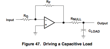
- Capacitive loading instability -- Opamp performance is usually specified with a resistive load. With a capacitive load, the op-amp's output resistance forms a low-pass-filter that reduces the op-amp's margin against instability. Sometimes an op-amp datasheet will discuss this and recommend that you put a small resistor (20-100 ohms) between op-amp output and any capacitive load more than a few picofarads. (The TLC081 datasheet mentions this on p. 16.) If you do this, you need to be careful how you connect the op-amp feedback. You can't take it only from the capacitive load, because the series resistance you've added will make the problem worse. One way is to take your feedback from before the small resistor (figure from the TLC081 datasheet):
Alternatively, you can use a "dual feedback" technique and take DC feedback from the capacitive load and high-frequency feedback directly from the op-amp output (figure from Analog Devices):
In any case, there are several good application notes on driving capacitive loads. Here's one from TI, one from Microchip, and one from Analog Devices.

- RF rectification -- This is an important gotcha that you should know about. You won't often run into it except when amplifying thermocouple signals, or if your circuit is working in the presence of large amounts of noise. What happens is that at low frequencies the op-amp works nice and linearly, but at very high frequencies, parasitic parts of the input transistors act like diodes and rectify that RF energy into varying DC voltages that mysteriously show up in your circuit. Thermocouple amplifiers are the common place this shows up because of two things: they need high gain, and thermocouples are long wires that act as an antenna for noise. If you stick a small capacitor (100-10000pF) in parallel with the thermocouple amplifier inputs and the problem goes away, it is almost certainly RF rectification. Shunt capacitance and/or series inductance (via ferrite beads or common-mode chokes) will usually limit RF rectification from being a problem.
- "Saturation recovery" aka "Overload recovery" -- If your opamp stays in its linear range, the specs on gain-bandwidth and slew rate apply. Need a fast amplifier? Go find one that has a 10MHz or even a 100MHz bandwidth. But let that op amp saturate, and all of a sudden it may take some time to recover. Look at the LMV2011 datasheet -- it's a 3MHz GBW op-amp, but it has overload recovery time listed as typically 50msec. That's milliseconds, which is dreadfully slow compared with the linear response of this op-amp at a gain of 10 (bandwidth should be 300kHz) or even 1000 (where its bandwidth should be 3kHz). Be warned that saturation recovery can be a problem not only with high gain circuits where the output saturates, but also with precision rectifier or peak detector circuits like these, where the output has to swing back and forth when the external diode comes in and out of conduction:


Other references
I'm sure I've missed at least one or two other subtleties about op-amps, but that's all I can remember at the moment. Two really good references for understanding op-amps (as well as many other aspects of circuit design) are The Art of Electronics by Horowitz and Hill, and Troubleshooting Analog Circuits, by the late Bob Pease.
Good luck with your circuit designs, and remember this rule about working with op-amps: no gain, no pain!


- Comments
- Write a Comment Select to add a comment
To post reply to a comment, click on the 'reply' button attached to each comment. To post a new comment (not a reply to a comment) check out the 'Write a Comment' tab at the top of the comments.
Please login (on the right) if you already have an account on this platform.
Otherwise, please use this form to register (free) an join one of the largest online community for Electrical/Embedded/DSP/FPGA/ML engineers:


