


Lost Secrets of the H-Bridge, Part IV: DC Link Decoupling and Why Electrolytic Capacitors Are Not Enough
Those of you who read my earlier articles about H-bridges, and followed them closely, have noticed there's some unfinished business. Well, here it is. Just so you know, I've been nervous about writing the fourth (and hopefully final) part of this series for a while. Fourth installments after a hiatus can bring bad vibes. I mean, look what it did to George Lucas: now we have Star Wars Episode I: The Phantom Menace and Indiana Jones and the Kingdom of the Crystal Skull. But then again: look at Star Trek IV: The Voyage Home — not bad. Not as good as Wrath of Khan, but a lot better than the first and third Star Trek movies. And don't forget the Fourth Doctor, Tom Baker. Or the Three Musketeers — there were really four of them: Athos, Porthos, Aramis, and D'Artagnan. Or the Three Stooges: does anyone remember Shemp? Well, he was one of the original Three Stooges, along with Moe and Larry, until Shemp quit and got replaced by Curly. Curly was Number Four! Woohoo!
So let's press on with our fourth installment of the H-bridge series. Without further ado:

Remember this diagram? The stuff on the right is the H-bridge, with four transistors switching on and off with pulse-width modulation. A relatively steady current IL flows through the load, with some ripple current at harmonics of the switching carrier frequency. For part of the switching cycle, the load current flows through the capacitor on the DC link as well. We need a capacitor as a local reservoir of charge, because the voltage source supplying the DC link comes from somewhere else, and there is quite a bit of series inductance. Good power supply designs don't just have one capacitor, they usually have at least three, and it's because of series inductance. Keep that in the back of your brain.
In the first three articles I talked about ripple current:
- Part I: analysis of load current ripple
- Part II: analysis of DC link current ripple
- Part III: practical aspects of inductor and capacitor ripple current
And I went through a whole bunch of equations and graphs like this:
Basically the load current has a sawtoothy look to it. Load current is fairly continuous. But the DC link current is pulsy, with lots of edges. Step changes in currents do not play well with series inductance. The inductance looks essentially like an open circuit at short time scales, and if there's nowhere for step changes in current to go, they create big voltage spikes.
# Ugh, another bunch of Python code to help simulate what's going on
# Some of these simulations take a long time to run, especially the later ones
# Skip this stuff if you're not interested

import numpy as np
import matplotlib.pyplot as plt
import matplotlib.gridspec as gridspec
import scipy.integrate

def sawtooth(t): return 1-abs(2*(t % 1) - 1)
def edges(tmin, tmax, D, fsw):
    phi0 = (1-D)/2.0
    phi1 = (1+D)/2.0
    def g():
        k0 = tmin*fsw
        k1 = tmax*fsw
        for k in np.arange(np.floor(k0),np.ceil(k1)):
            for phi in (k+phi0, k+phi1):
                if phi >= k0 and phi <= k1:
                    yield phi/fsw
    return list(g())

fsw = 10e3
t = np.arange(0,2,0.0001)/fsw
u_Icdc = lambda t: ((sawtooth(2*fsw*t) > 0.4) - 0.6)*3
u_Icdc.crit = lambda tmin, tmax: [tmin]+edges(tmin, tmax, 0.6, 2*fsw)

class VSource(object):
    def rawresponse(self,t,Is):
        trange = (min(t),max(t))
        try:
            tcrit = Is.crit(trange[0],trange[1])
        except:
            tcrit = None
        return scipy.integrate.odeint(self.dydt, self.get_y0(), t, args=(Is,), tcrit=tcrit, **self.odeargs())
    def response(self,t,Is):
        return self.rawresponse(t,Is)
    def dydt(self, y,t0,Is):
        pass
    def odeargs(self):
        return {}

class VSource1Plain(VSource):
    '''just an ideal capacitor'''
    def __init__(self,c):
        self.capacitance = c
    def response(self,t,Is):
        return -scipy.integrate.cumtrapz(Is(t),t,initial=0)/self.capacitance

def describe(item):
    k = int(np.floor(np.log10(item)/3))
    r = item / (10 ** (3*k))
    try:
        suffix = ['p','n','$\\mu$','m','','k','M','G'][k+4]
    except:
        suffix = ''
    return ('%.1f' % r)+suffix

def vvect(v):
    return np.array([v]).transpose()

class VSource1(VSource):
    '''just an ideal capacitor'''
    def __init__(self,C):
        self.capacitance = C
    def dydt(self,y,t0,Is):
        return -Is(t0)/self.capacitance
    @property
    def ylabels(self):
        return ['$\\Delta V_{DC}$']
    @property
    def title(self):
        return 'ideal capacitor %sF' % describe(self.capacitance)
    def get_y0(self):
        return 0

class VSource2(VSource):
    '''capacitor + Ls'''
    def __init__(self,C,Ls,Rs=0):
        self.capacitance = C
        self.Ls = Ls
        self.Rs = Rs
    def response(self,t,Is):
        r = self.rawresponse(t,Is)
        Icap = vvect(Is(t)-r[:,1])
        return np.hstack((r,Icap))
    def dydt(self,y,t0,Ilink):
        Is = y[1]
        dVdt = (Is-Ilink(t0))/self.capacitance
        dIdt = (-Is*self.Rs - y[0])/self.Ls
        return (dVdt, dIdt)
    @property
    def ylabels(self):
        return ['$\\Delta V_{DC}$','$\\Delta I_s$','$I_{cap}$']
    @property
    def title(self):
        items = tuple(describe(x) for x in (self.capacitance, self.Rs, self.Ls))
        return 'ideal capacitor %sF, source impedance = %s$\\Omega$ + %sH' % items
    def get_y0(self):
        return (0,0)


def plotit(t,u_Icdc,Vs,tzoom=None):
    fig = plt.figure(figsize=(8,6))
    r = Vs.response(t,u_Icdc)
    n = r.shape[1]
    assert n < 10
    if tzoom and hasattr(u_Icdc,'crit'):
        nx = 2
        width_ratios = [3,1]
        izoom = np.where((t >= tzoom[0]) & (t <= tzoom[1]))
    else:
        nx = 1
        width_ratios = [1]
    gs = gridspec.GridSpec(n+1, nx,
                       width_ratios=width_ratios,
                       wspace = 0.05, hspace=0.1)


    ax = fig.add_subplot(gs[0,0])
    ax.plot(t*1e6,u_Icdc(t))
    ax.set_ylim(-3.3,2.2)
    if n > 0:
        ax.set_xticklabels([])
    ax.set_ylabel('$\\Delta I_{DClink}$', fontsize=17)

    if tzoom:
        ax = fig.add_subplot(gs[0,1])
        ax.plot(t[izoom]*1e6,u_Icdc(t[izoom]))
        ax.set_ylim(-3.3,2.2)
        ax.set_yticklabels([])
        if n > 0:
            ax.set_xticklabels([])
        xzlim=(tzoom[0]*1e6,tzoom[1]*1e6)
        ax.set_xlim(xzlim)

    ylabels = Vs.ylabels
    for i in range(n):
        ax = fig.add_subplot(gs[i+1,0])
        y = r[:,i]
        ax.plot(t*1e6,y)
        if i < n-1:
            ax.set_xticklabels([])
        ax.set_ylabel(ylabels[i], fontsize=17)
        if i == 0:
            k = np.argmax(np.abs(y))
            tk = t[k]*1e6
            ax.plot(tk, y[k], '.')
            ax.annotate('%.2f' % y[k],
                xy=(tk, y[k]), xycoords='data',
                xytext=(tk, 0), textcoords='data',
                bbox=dict(boxstyle="round", fc="w"),
                arrowprops=dict(arrowstyle="->",
                                connectionstyle="angle3,angleB=90,angleA=180"
                                ),
            )
        yzlim = ax.get_ylim()
        if tzoom:
            ax1 = fig.add_subplot(gs[i+1,1])
            ax1.plot(t[izoom]*1e6,y[izoom])
            ax1.set_xlim(xzlim)
            ax1.set_ylim(yzlim)
            ax1.set_yticklabels([])
            if i < n-1:
                ax1.set_xticklabels([])

    ax.set_xlabel('time (microseconds)')
    fig.suptitle(Vs.title)
Let's look at an example with some real numbers.
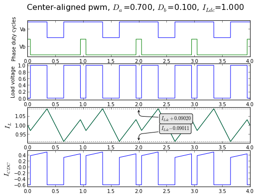
Suppose I have an H-bridge that I want to run off 36V, and deliver up to 3A load current. I want to use center-aligned PWM with a switching frequency of 10kHz. I'll also use a common-mode duty-cycle of 0.5, so my ripple currents will have harmonics of 20kHz, but no content at the 10kHz switching frequency. I have a high enough load inductance that my output ripple current is small, and doesn't add much content to the DC link waveform.
Okay: first, we need to find a capacitor that can handle at least 1.5ARMS ripple current at 20kHz. (See part III under "Ripple current in the DC link capacitors", if you don't remember that for low ripple current in the load, the graph of RMS current in the DC link capacitor vs. duty cycle is a semicircle, with a maximum of half the DC load current at 50% duty cycle.)
Let's say I do a little bit of pencil and paper analysis, and I think that a 470uF 63V capacitor is a good match, and I find the Panasonic EEUFC1J471L. The datasheet has some information on it:
- 12.5mm diameter
- 30mm length
- 2090mA max RMS ripple current at 100kHz (derated at 10kHz to 95% = 1985mA)
- 55 mΩ max impedance at 100kHz
Looks good! Let's see what an ideal 470uF capacitor does with a 60% differential duty cycle (one leg of the H-bridge switching at 20%, the other at 80%):
Vs1 = VSource1(470e-6)
tzoom = (9.8e-6,11.8e-6)
plotit(t,u_Icdc,Vs1,tzoom=tzoom)
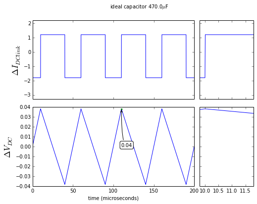
Not bad — only about 80mV peak-to-peak ripple.
Oh wait — we forgot about our voltage source. What effect does the voltage source have with series resistance and inductance? Here's a graph of a simulation with a voltage source that has 5mΩ series resistance and 5nH series inductance. This is a ridiculously low inductance, but let's just see what it looks like.
Vs2 = VSource2(470e-6, 5e-9, 0.005)
plotit(t,u_Icdc,Vs2,tzoom=tzoom)
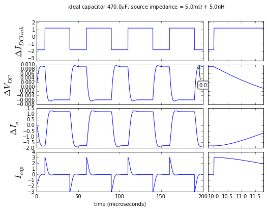
Here most of the DC load current flows directly from the voltage source; the capacitor is helping supply the current to the DC link only for the first few microseconds. And the DC voltage ripple depends mostly on the series resistance of the voltage source. But again, 5nH series inductance is ridiculously low. A more reasonable number is 1μH:
Vs2 = VSource2(470e-6, 1e-6, 0.005)
plotit(t,u_Icdc,Vs2, tzoom=tzoom)
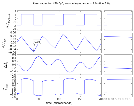
Here we are actually getting a little bit of resonance between the DC link capacitance and the source inductance. But most of the source ripple current is coming from the DC link capacitor now. Which is what we want, anyway: this ripple current is at 20kHz and can cause EMI problems if it's zipping across some wires.
At 5μH the resonance is still there, but the ripple current from the supply is essentially negligible:
Vs2 = VSource2(470e-6, 5e-6, 0.005)
plotit(t,u_Icdc,Vs2,tzoom=tzoom)
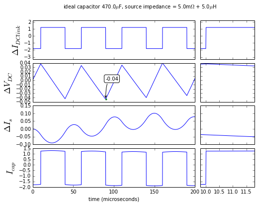
From here on out we'll just neglect the voltage source, and pretend it has high inductance so we have to handle the DC link ripple current via our DC link capacitor.
Okay, the next reality check is the DC link capacitor ESR. Our Panasonic 470μF capacitor doesn't have a direct specification for ESR. Not many electrolytic capacitors do, presumably because it's hard to test. We do have something in the datasheet called the loss tangent. The 63V capacitors have a maximum loss tangent of 0.08, measured at 120Hz. We can calculate ESR \( = \frac{\tan \delta}{\omega C} = \frac{0.08}{2\pi \cdot 120 \text{Hz} \cdot 470 \mu F} = 0.23\Omega \), but this isn't a very tight specification. There is a spec on impedance at 100kHz of 55mΩ, but we don't know whether that's due mostly to ESR or ESL. I really wish capacitor manufacturers would give more detailed component data, but they generally don't.
Let's take a look at some different series of capacitors. The Vishay 136 RVI series is very low ESR, and has a 470uF 63V part, but it's only rated at 1500mA RMS — no margin left over. Still, there's one important thing about this datasheet — it has an impedance vs. frequency graph:
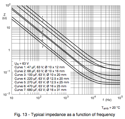
At low frequencies, the capacitor looks... well... capacitive. But there's that knee in the curve, and in the 10-100kHz range, it flattens out. At a higher frequency, the curve will bend upwards due to parasitic inductance. But the graphs don't go any higher in frequency.
Anyway, let's go back to the Panasonic 470uF capacitor (EEUFC1J471L), assume the 55mΩ impedance is all ESR, and plug it into a simulation:
class VSource3(VSource):
    '''capacitor + ESR'''
    def __init__(self,C,ESR=0):
        self.capacitance = C
        self.R = ESR
    def response(self,t,Is):
        r = self.rawresponse(t,Is)
        Vcap = r[:,0]
        return vvect(Vcap - Is(t)*self.R)
    def dydt(self,y,t0,Ilink):
        dVdt = -Ilink(t0)/self.capacitance
        return dVdt
    @property
    def ylabels(self):
        return ['$\\Delta V_{DC}$']
    @property
    def title(self):
        items = tuple(describe(x) for x in (self.capacitance, self.R))
        return 'ideal capacitor %sF, ESR = %s$\\Omega$' % items
    def get_y0(self):
        return (0,0)

Vs3 = VSource3(470e-6, 55e-3)
plotit(t,u_Icdc,Vs3,tzoom=tzoom)
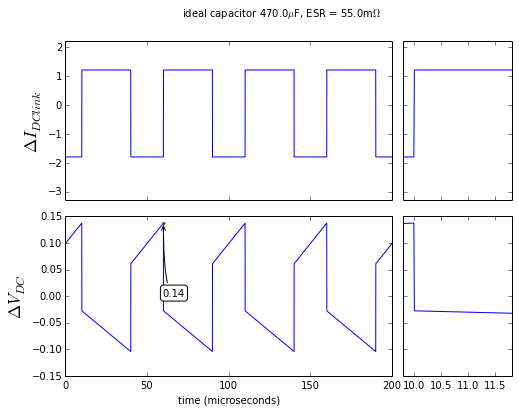
You can see the ESR increases the voltage ripple on the DC link. Not awful but it's definitely worse than before. What will really mess things up is the series inductance. We'll see a huge spike on the DC link. If there is no other capacitance on the DC link, we'll get an infinite voltage spike in response to a current step. That's not realistic, though, because there's always other sources of parasitic capacitance.
I've only found a few electrolytic capacitor datasheets that mention series inductance or ESL. The EPCOS B41793 series and the Cornell Dubilier 350 series both have three pins for rugged mounting and low ESL, only about 10nH. Cornell Dubilier's 301 series claims series inductance in the 12-16nH range; the 470 63V capacitor (part #301R471M063FF2) is rated at 3.27A RMS ripple at 20kHz and has a max ESR of 43 mΩ.
Let's try simulating the Cornell Dubilier 301 series capacitor. We'll give them benefit of the doubt and say that it's 12nH ESL. And just to handwave things, let's assume there's about 100pF of parasitic capacitance elsewhere on the DC link:
# Here is some code for simulating a group of capacitors with ESL and ESR,
# along with a single capacitor representing parasitic capacitance

class VSourceCList(VSource):
    '''base class for N capacitors with ESL and ESR, plus plane capacitance'''
    def __init__(self,ncaps,Clist,ESRlist,ESLlist,nlist,Cplane,odeargs=None):
        self.ncaps = ncaps
        assert len(Clist) == ncaps
        assert len(ESRlist) == ncaps
        assert len(ESLlist) == ncaps
        assert len(nlist) == ncaps
        self.C = tuple(Clist)
        self.R = tuple(ESRlist)
        self.L = tuple(ESLlist)
        self.N = tuple(nlist)
        self.Cplane = Cplane
        self._odeargs = {} if odeargs is None else odeargs
    def response(self,t,Ilink):
        r = self.rawresponse(t,Ilink)
        Icplane = -Ilink(t)
        for k in range(self.ncaps):
            Icplane -= r[:,k+1]
        return np.hstack([r[:,:(self.ncaps+1)], vvect(Icplane)])
    def dydt(self,y,t0,Ilink):
        V = y[0]
        Icplane = -Ilink(t0)
        n = self.ncaps
        result = [0]*(2*n+1)
        for k in range(n):
            Ic = y[k+1]
            Vc = y[k+1+n]
            Icplane -= Ic
            Nk = self.N[k]
            C = self.C[k]*Nk
            R = self.R[k]/Nk
            L = self.L[k]/Nk
            # dVc/dt:
            result[k+1+n] = Ic/C
            # dIc/dt:
            result[k+1] = (V - Vc - Ic*R)/L
        # dV/dt for the plane capacitor across the DC link:
        result[0] = Icplane/self.Cplane
        return result
    @property
    def ylabels(self):
        return ['$\\Delta V_{DC}$']+['$I_{C%d}$' % (k+1) for k in range(self.ncaps)]+['$I_{Cp}$']
    def getTitleParts(self):
        s = []
        for k in range(self.ncaps):
            Nklabel = '' if self.N[k] == 1 else '%dx' % self.N[k]
            items = tuple(describe(x) for x in [self.C[k], self.R[k], self.L[k]])
            s.append('C%d = %s %sF, ESR = %s$\\Omega$, ESL = %sH' % (k+1,Nklabel,items[0],items[1],items[2]))
        s.append('Cp = %sF' % describe(self.Cplane))
        return s
    def get_y0(self):
        return tuple([0]*(2*self.ncaps + 1))
    @property
    def title(self):
        seplist = [' %s']*(self.ncaps+1)
        seplist[(self.ncaps+1)//2] = '\n%s'
        format_string = 'Capacitor' + ';'.join(seplist)
        return format_string % tuple(self.getTitleParts())
    def odeargs(self):
        return self._odeargs
Vs4 = VSourceCList(1,
Clist=[470e-6],
ESRlist=[43e-3],
ESLlist=[12e-9],
nlist=[1],
Cplane=100e-12,
odeargs=dict(atol=100e-6))
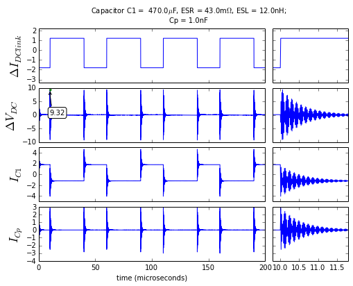
plotit(t,u_Icdc,Vs4,tzoom=tzoom)

OUCH! Those are 30V spikes! See what happens when you try to switch on and off a current with nowhere to go but an inductive load and an itty-bitty capacitor? The capacitors sing like a tuning fork. Let's try increasing our parasitic capacitance from 100pF to 1000pF:
Vs4 = VSourceCList(1,
                   Clist=[470e-6],
                   ESRlist=[43e-3],
                   ESLlist=[12e-9],
                   nlist=[1],
                   Cplane=1000e-12,
                   odeargs=dict(atol=100e-6))
plotit(t,u_Icdc,Vs4,tzoom=tzoom)
Even here, we have 10V spikes. It would be nice if we could find a low-impedance capacitor, since the electrolytic capacitor's series inductance is causing us a bunch of trouble.
Wishing Will Make It So: Embedded Capacitance in Printed Circuit Boards
Say no more! We do have access to a low-impedance capacitor. Copper planes on a printed circuit board make an excellent parallel-plate capacitor, that acts "capacitive" up to tens or even hundreds of megahertz, with low ESR and low parasitic inductance. But we have to sharpen our pencils and figure out how to do it.
Step 1: Physics
First, we have to remember the formula for capacitance of a pair of parallel plates, \( C = \frac{\epsilon A}{d} \), where A is the plate area, d is the distance between plates, and ε is the dielectric permittivity. Air and vacuum have a permittivity of 8.85 pF/m: if we had a pair of square conductive plates in air that were 2.5mm apart, with side 5cm, then we/d have \( C = 8.85\text{pF/m} \times \frac{(0.05m)^2}{0.0025m} = 8.85\text{pF} \).
8.85pF? That's it?!?! Yep. Parallel plates make great capacitors, but their capacitance is really small unless the area is really large or the spacing is small. The good news is that with printed circuit boards, we can have small spacings, and the dielectric material isn't air. Many circuit boards are manufactured using the FR-4 dielectric, which has a relative permittivity of 4.8, so ε(FR4) = 42.5pF/m.
Step 2: PCB layer stackups
OK, so here's where things get a little tricky.
PCB design involves two major steps: schematic design and PCB layout. The schematic design is the higher-level part: poof! add a resistor and a capacitor and connect them together. Tada! Instant low-pass filter. The layout step is full of grungework. On the one hand, you can bulldoze your way through it, or use an auto-routing tool and let the computer do the dirty work... but in the process you're likely to miss a few important design decisions. On the other hand, you can try to handle each and every step carefully, and spend days agonizing about ten thousand different choices, getting it perfect... in which case you're likely to miss a few important design decisions. The key to being good at PCB layout is to partition the problem into the 100 important choices and the 9,900 unimportant choices, then bulldoze through the unimportant ones and treat the 100 important choices with utmost care.
I found out early on that PCB layout is not my forte. The last PCB layout I worked on all by myself was in 1998 or 1999; it was a battery gauge board about 1cm × 4cm in size, with only 3 ICs and a dozen or so passive components. I worked on it for a few weeks, trying to be a perfectionist; by the end of the project I realized I stopped looking at the circuit board as a battery gauge, and instead as a 4-layer rectangle with lots of little copper rectangles trying to twist their way around each other to get from point A to point B. And that was enough for me — time to retire my career as a solo PCB layout designer.
Since then, I've learned to work with specialists. They know how to do most of the work very well on their own. They work with the little copper rectangles, mostly without knowing too much about the schematic, and I step in when there's some critical issues to worry about. The specialists do their job, push a button, and zing! out come the Gerber files, those ubiquitous vector graphics files that PCB houses use with photolithography to etch and assemble the copper layers of a circuit board
One of the design decisions you make in PCB design has almost nothing to do with the PCB layout software. The bulk of the layout work is defining component footprints, choosing proper component placement, and creating copper traces and vias in the right spots. But someone also has to make a decision about the PCB layer stackup. The circuit board is a sandwich of conductors and insulators. Even a simple 4-layer board has lots of choices. How thick is the copper on each layer? How thick is the dielectric insulation between layers? What type of dielectric insulation is used? Which order are the layers placed in? Fortunately, the PCB houses have some good default guidelines. Just make sure you explicitly call out the layer stackup: what you don't want is for some of the important design decisions to be left up to the PCB manufacturer, so that batch 1 from manufacturer 1 has a significant difference from batch 2 from manufacturer 2.
Anyway, take this advice with a grain of salt: I know the basics of PCB layout, but I'm not an expert, and if you really need something done precisely, talk to a PCB design guru.
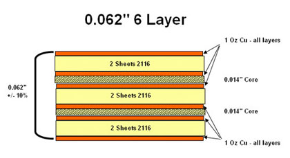
As far as the basics of layer stackups: Advanced Circuits is a popular US circuit board manufacturer for electronics prototyping, and their website lists a number of common layer stackups. Here's a typical 4-layer 0.062" board, shown on the Advanced Circuits website:

You'd probably choose the outer layers for signals and the two inner layers for power planes. The distance d between the planes in that case would be 40 mils or 1.02mm. This takes up most of the thickness; the 0.062" board is 1.57mm thick; each 1oz copper layer is only 0.035mm thick. That leaves about 0.20mm for each of the 2116 laminates.
Let's say we had a 5cm × 10cm area for a power and ground plane. Then with a 1.02mm FR-4 dielectric, our inter-plane capacitance would be 42.5pF/m × 5cm × 10cm / 1.02mm = 208pF. Not bad for free capacitance. Or we could design the layer stackup more explicitly for embedded capacitance, using either a thinner dielectric or a material with higher permittivity.
Or we could specify a 6-layer board, and use 4 layers for planes in the area of the H-bridge — with 2 plane layers and 2 extra signal layers in the rest of the board. After all, power semiconductor circuitry usually isn't densely laden with signals, at least not the way analog or digital circuits are usually designed.
Here's a 6-layer 0.062" board stackup from the Advanced Circuits website:
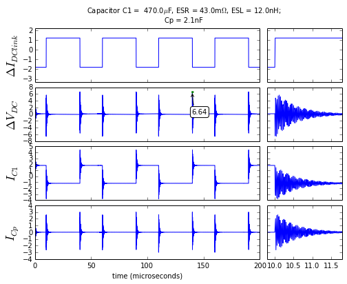
If we used a layer stackup of Signal1 | Ground | DC+ | DC+ | Ground | Signal2, this would give us two inter-plane capacitances each with 0.014" = 0.36mm; a 5cm × 10cm area would give us C = 2 × (42.5pF/m × 5cm × 10cm / 0.36mm) = 2 × 590pF = 1180pF. Plus we get reduced series resistance and inductance for the critical power circuitry, since the DC+ and Ground nodes each have two planes in parallel.
Or we could use Signal1 | Ground | DC+ | Ground | DC+ | Signal2, with the disadvantage that Signal2 couples closely to DC+ rather than Ground. But this has an additional capacitance between the two inner layers. If you do the math on the board layer thicknesses, the two inner planes are about 0.22mm apart in distance, which means the inner DC+ and Ground form another capacitor with C = 42.5pF/m × 5cm × 10cm / 0.22mm = 966pF. Total capacitance is 2 × 590pF + 966pF, for a total of 2146pF. Now we're down to 6.6V spikes on the DC link:
Vs4 = VSourceCList(1,
                   Clist=[470e-6],
                   ESRlist=[43e-3],
                   ESLlist=[12e-9],
                   nlist=[1],
                   Cplane=2146e-12,
                   odeargs=dict(atol=100e-6))
plotit(t,u_Icdc,Vs4,tzoom=tzoom)
We could go further with specialized circuit board materials and processes, such as 3M's Embedded Capacitance Material; C0614 has a relative permittivity of 16 and a controlled distance between planes of only 14um, for a capacitance of 1000pF/cm2. A 5cm x 10cm section of C0614 ECM would yield C = 50,000pF:
Vs4 = VSourceCList(1,
                   Clist=[470e-6],
                   ESRlist=[43e-3],
                   ESLlist=[12e-9],
                   nlist=[1],
                   Cplane=50000e-12,
                   odeargs=dict(atol=100e-6))
plotit(t,u_Icdc,Vs4,tzoom=tzoom)
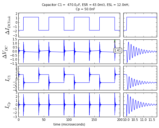
We're down to about 1.4V spikes. But that's still pretty noisy, and now we have to use special circuit board fabrication techniques, which means higher cost and fewer choices of vendors. Note in particular that the 470uF capacitor and the plane capacitance are fighting each other: the capacitors are resonating and current sloshes back and forth between the two capacitors, with even higher current than we're switching from the H-bridge. This is a sign that maybe we're doing something wrong. What could it be?
Goldilocks and the Three Capacitors
This issue really boils down to a mismatch:
- We have a nice big 470uF aluminum electrolytic capacitor, for bulk capacitance, that can support the ripple current at the switching frequency — but it has inductance that prevents it from being effective at much more than 100kHz.
- We have a great high-frequency capacitor in the power planes of a printed circuit board, but it's only in the 1000-5000pF range without special PCB construction.
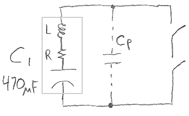
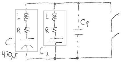
While we could increase the electrolytic capacitance, by using larger capacitors or several in parallel, the better approach is to use a third capacitor, C2 in the diagram below, with a value that is something in between the electrolytic capacitor C1 (TOO BIG) and the PCB plane capacitance Cp (TOO SMALL). We want a good high-frequency bypass capacitor: either a film or ceramic capacitor (JUST RIGHT!).
For lower voltage systems (100V or less), ceramic capacitors are generally the best choice. Above 100V, ceramic capacitors are harder to find, and film capacitors are usually a better option.
These high frequency capacitors are bypass capacitors, and should be placed as close as possible to each half bridge to minimize the loop area of switching transients. In fact, for higher-power systems, there are special packages for film capacitors designed to mount directly onto IGBT modules:

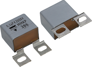
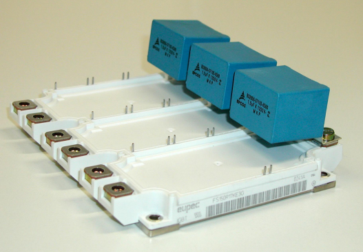

These are designed to minimize both parasitic inductance and loop area, and are available from several manufacturers: Aerovox, Cornell Dubilier, Electronics Concepts, Illinois Capacitor, Kemet, Vishay, and WIMA, for example.
The capacitors are meant to be placed across the terminals of a module (images from the WIMA GmbH website) or onto bus bars:


In our 36V H-bridge, ceramic capacitors would do the trick. The Murata GRM32ER71H475KA88 is a 4.7uF 50V 1210 ceramic capacitor with the following impedance vs. frequency chart:

This kind of chart makes it very easy to determine circuit parameters. We know C = 4.7uF, and the dip in the resonance curve at 2.5MHz tells us the ESR is about 5 mΩ. The capacitor impedance at high frequencies is about 0.2Ω at 100MHz and 2Ω at 1GHz. With \( Z_L = j\omega L \), this means that L ≈ 0.32nH. Ordinarily that would mean a resonant frequency of \( f = \frac{1}{2\pi\sqrt{LC}} \) ≈ 4.1MHz, not 2.5MHz, but there's a funny change of resistance vs. frequency near resonance, that shifts the notch in the impedance curve.
Well, great! We'll use some of these capacitors, and they only have 0.32nH of parasitic inductance.
There's one catch, though: 0.32nH is the intrinsic inductance of the capacitors. We can come close to this value, but not quite as low, because the inductance of the connections to the planes is significant compared to the intrinsic inductance of the capacitor. If we do a good job with connecting vias to the planes, we might be able to have the total series inductance be on the order of 1nH.
In any case, let's use two of these capacitors, one for each half-bridge, and see what happens to our DC link voltage:
Vs5 = VSourceCList(2,
                   Clist  =[470e-6,4.7e-6],
                   ESRlist=[43e-3, 5.0e-3],
                   ESLlist=[12e-9, 1.0e-9],
                   nlist=[1,2],
                   Cplane=2146e-12,
                   odeargs=dict(atol=100e-6))
plotit(t,u_Icdc,Vs5,tzoom=tzoom)
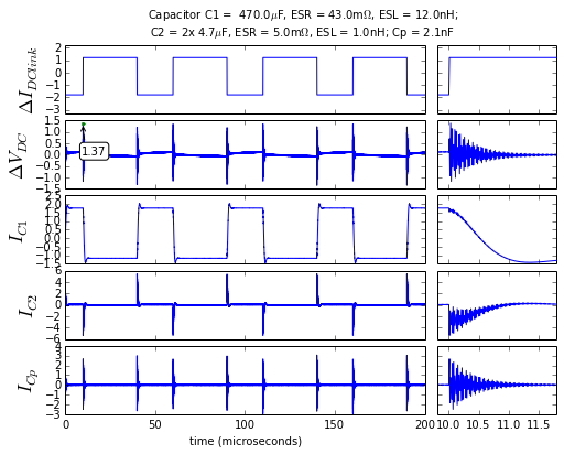
Hey, that's only 1.37V! That's even better than the special embedded capacitor circuit board.
Maybe we can do a little bit better: we still have a big gap in capacitance between the 2.1nF of the power planes, and the 9.4uF of the ceramic capacitors.
Why don't we add a fourth capacitor, C3?
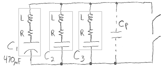
We could use a bunch of 0.01uF capacitors in parallel. They're cheap and common. Let's try 6 of them on each half-bridge, for a total of 12, to keep the net inductance low and share current among them. The Murata GRM188R71H103KA01 is a 0.01uF 50V 0603 capacitor, that costs less than 0.5 cents apiece from Digikey in quantity 1000, and has this impedance vs. frequency plot:

Looks like 0.1Ω ESR, and a quick calculation using 3Ω impedance at 1GHz yields about 0.5nH in intrinsic inductance of the capacitor. There are a few things to note about the inductance of passive components.
- If the component is well utilized, this intrinsic inductance is more related to the geometry of the package itself rather than the component. In other words, unless we've got a crappy capacitor, all capacitors in 0603 packages will have about the same intrinsic inductance.
- The smaller the loop area, and the smaller the package, the lower the inductance. We could have used an 0402 package: as you can see from the graph below, the GRM155R71H103KA88 has about 1.8Ω impedance at 1GHz, for an intrinsic inductance of 0.3nH. But it's slightly more expensive, and we're still going to be limited by the via inductance we can use to get to the ground plane more than the intrinsic inductance itself.

- Through-hole components suck! No, really, avoid them like the plague. Feel free to use them in your early prototyping, but when you start to get serious, if you care at all about high-frequency characteristics, stick with surface-mount. The component leads alone in through-hole components add a lot of parasitic inductance. There are exceptions to this rule (e.g. increased voltage clearance, better ability to handle the stresses of board flexure) but they're just that: exceptions.
The ultimate in low-inductance SMT packages are the so-called "reversed-geometry" packages, e.g. 0306 instead of 0603, where the component leads are on the long edge of the package rather than the short edge. For example the LLL185R71E103MA01 has an impedance of only about 0.5Ω at 1GHz (less than a third of the 0402 package inductance!) — but the highest rated voltage for a 0.01uF capacitor in this package is only 25V, and because the 0306 package is less commonly used than the regular 0603 package, it costs a whopping 7 cents apiece in quantity 1000 from Digikey. Still, if you're doing RF design and need to get something to work well in the gigahertz range, these types of packages are available.
All right, let's simulate the 0.01uF capacitors:
Vs6 = VSourceCList(3,
                Clist  =[470e-6, 4.7e-6, 0.01e-6],
                ESRlist=[43e-3,  5e-3,  0.1],
                ESLlist=[12e-9,  1e-9,  1e-9],
                nlist  =[1,2,12],
                Cplane=2146e-12,
                odeargs=dict(atol=100e-6))
plotit(t,u_Icdc,Vs6,tzoom=tzoom)
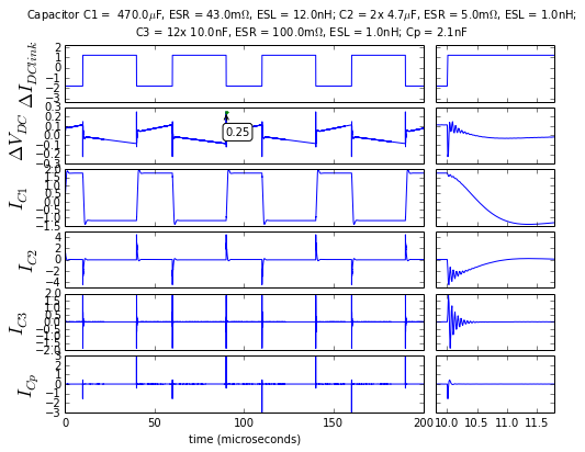
Ooh! Even better: 0.25V ripple. Now, notice that the resonance is happening between C2 and C3: the currents in C1 and the plane capacitance are relatively quiet. So we could try swapping some of the 0.01uF capacitors for 0.1uF capacitors, to fill some of the gap between C2 and C3. Let's take a look at the GRM188R71H104KA93, a 0.1uF 50V 0603 capacitor (1 cent apiece in qty 1000 from Digikey):

You know the drill: 20mΩ ESR, 1.8Ω at 1GHz → 0.3nH series inductance. Let's go:
Vs7 = VSourceCList(4,
                Clist  =[470e-6, 4.7e-6, 0.1e-6, 0.01e-6],
                ESRlist=[43e-3,  5e-3,  20e-3, 0.1],
                ESLlist=[12e-9,  1e-9,  1e-9, 1e-9],
                nlist  =[1,2,4,8],
                Cplane=2146e-12,
                odeargs=dict(atol=50e-6))
plotit(t,u_Icdc,Vs7,tzoom=tzoom)
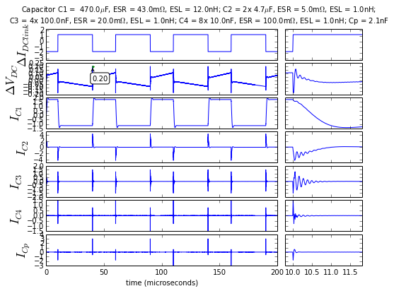
Not much better, unfortunately. Oh well. If we look at the zoomed-in plot of voltage ripple, we see the spike right at the switching instant, and that means that the bulk of the noise spikes are determined by the really high-frequency components, namely the 0.01uF capacitors and the plane capacitance.
Also let's look how the currents are shared: The 470uF bulk capacitor handles the low-frequency current, and sees almost all of the RMS current ripple. The 4.7uF ceramic capacitor provides some charge for the first microsecond or so: ironically in the opposite direction of the load current, so it's really there to null out some of the noise spikes rather than provide current to the load. The 0.1uF and 0.01uF capacitor currents handle transients at shorter and shorter timeframes, with the plane currrent itself handling the very high frequency transients.
Please realize that this is only an approximate simulation. Real H-bridges have finite switching times, so the currents pulled from the DC link are not perfect square waves, but rather more like trapezoids with slew-rate-limited edges. Also these simulations assume lumped-parameter models and ignore transmission line effects, along with the funky frequency-dependent resistances of the capacitors as described in their datasheets. But it's useful to understand the principles involved, even if the results are not perfect.
Frequency analysis
Another way to look at the results is to view the impedance of our composite voltage source in the frequency domain. This is a bit easier to compute, and lends insight, even if it doesn't yield answers on how much voltage ripple we can expect.
In fact, it's so easy we can make ourself a mini-framework to help compute it:
class TwoTerminal(object):
'''devices with two terminals'''
def __or__(self, other):
return Parallel(self, other)
def __add__(self, other):
return Series(self, other)
class Parallel(TwoTerminal):
def __init__(self, *objects):
def helper(objects):
for obj in objects:
if isinstance(obj, Parallel):
for o2 in obj.components:
yield o2
else:
yield obj
self.components = tuple(helper(objects))
def impedance(self, s):
'''compute the parallel combination of impedances'''
Y = 0
for obj in self.components:
Y += 1.0/obj.impedance(s)
return 1.0/Y
class Series(TwoTerminal):
def __init__(self, *objects):
def helper(objects):
for obj in objects:
if isinstance(obj, Series):
for o2 in obj.components:
yield o2
else:
yield obj
self.components = tuple(helper(objects))
def impedance(self, s):
'''compute the series combination of impedances'''
Z = 0
for obj in self.components:
Z += obj.impedance(s)
return Z
class Resistor(TwoTerminal):
def __init__(self,R):
self.R = R
def impedance(self,s):
return np.ones_like(s)*self.R
class Inductor(TwoTerminal):
def __init__(self,L,R=None):
self.L = L
self.R = R
def impedance(self,s):
'''the impedance at various frequencies.'''
Z = self.L*s
if self.R is not None:
Z += self.R
return Z
class Capacitor(TwoTerminal):
def __init__(self,C,R=None,L=None,n=1):
self.C = C
self.R = R
self.L = L
self.n = n
def impedance(self,s):
'''the impedance of a capacitor with ESR and ESL at various frequencies.
n = the number of capacitors in parallel'''
Z = 1.0/self.C/s
if self.R is not None:
Z += self.R
if self.L is not None:
Z += self.L*s
return Z/self.n
def Zparallel(Zlist):
Y = 0
for Z in Zlist:
Y += 1.0/Z
return 1.0/Y
def loop(x):
while True:
yield x
def plot_impedance(f, components, fmt=None, fig=None):
s = 2.0j * np.pi * f
if fig is None:
fig = plt.figure(figsize=(8,6))
if fmt is None:
fmt = loop(None)
ax = fig.add_subplot(1,1,1)
for (c, fmt_k) in zip(components, fmt):
args = [] if fmt_k is None else [fmt_k]
ax.loglog(f,np.abs(c.impedance(s)),*args)
ax.grid(which='major', color='black', linestyle='-')
ax.grid(which='minor', color='gray', linestyle='-')
ax.set_ylabel('impedance, ohms')
ax.set_xlabel('frequency, Hz')
return ax
log_f = np.linspace(-1,10,501)
f = 10 ** log_f
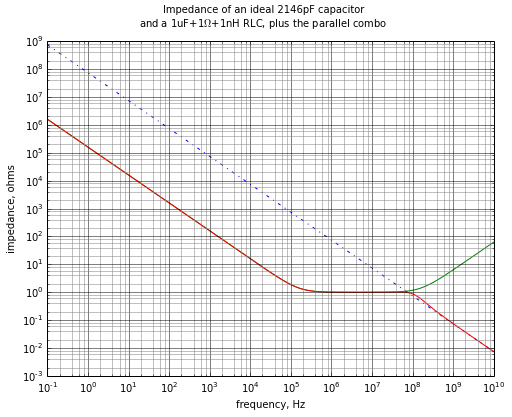
Cplane = Capacitor(2146e-12)
Ctest = Capacitor(1e-6) + Resistor(1) + Inductor(1e-9)
ax = plot_impedance(f, [Cplane, Ctest, Cplane | Ctest], ['-.','-','red'])
ax.figure.suptitle('Impedance of an ideal 2146pF capacitor\nand a 1uF+1$\Omega$+1nH RLC, plus the parallel combo')
Sweet! This is going to be easy:
Cbulk = Capacitor(C=470e-6, R=43e-3, L=12e-9)
Chf1  = Capacitor(C=4.7e-6, R=5e-3,  L=1e-9, n=2)
Chf2  = Capacitor(C=0.01e-6, R=0.1,  L=1e-9, n=12)
Cplane = Capacitor(2146e-12)

ax = plot_impedance(f,[Cplane,Cbulk,Chf1,Chf2,
                       Cplane|Cbulk|Chf1|Chf2],['r','g','b','c','k'])
ax.legend(('2146pF plane','470uF','2x4.7uF','12x0.01uF','parallel combo'))
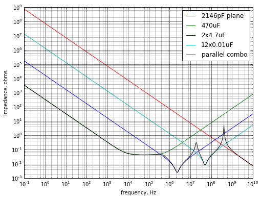
Great! We can see right away that there's a resonant peak at around 300MHz, formed by the resonance between the plane capacitance and the inductance of the 0.01uF capacitors. To improve things, one of five things has to happen at this point:
- We bite the bullet and pay for the expensive circuit board with higher plane capacitance
- We need to add something that has a lower impedance near the resonance (the only really practical solution here is to increase the number of 0.01 capacitors, and maybe use a variety of capacitor values so they smear out the resonant peak a little bit)
- The Real World has some unmodeled dynamics that help roll off the frequency response at frequencies above 100MHz and dampen that resonance
- The Real World has some unmodeled dynamics where the excitation source (our H-bridge) rolls off at frequencies above 100MHz, so the resonance isn't excited as much in the first place
- We decide that what we have is Good Enough!
Probably a combination of the last three will serve us. A 36V DC link for a power electronic circuit, with 0.25V spikes at the switching frequency, isn't too bad. Sensitive circuits will need to be isolated from this noise, via LC filters or ferrite beads, for example.
The real point here is that we were able to reduce the effect of switching noise from the H-bridge from 6.6V peak (with just the 470uF electrolytic capacitor + the 2146pF plane capacitance) to 0.25V peak, just by adding some relatively inexpensive and small capacitors, and understanding what's really happening in this situation. And that's powerful!
Summary and References
Okay, what have we learned today?
- Good power supply decoupling requires multiple capacitors in parallel, including bulk capacitance, high-frequency discrete capacitors, and PCB plane capacitance: no single capacitor is good enough to work well across a wide frequency range.
- It is vital to minimize parasitic inductance between capacitors and the power planes. This can be done through a combination of proper component selection, careful layout, and use of multiple parts in parallel.
- Bulk capacitors will help deliver current to a switching bridge at the carrier frequency, but not at much higher frequency. These capacitors bear the brunt of RMS ripple current.
- High frequency discrete capacitors are generally ceramic for low voltages (< 100V), and film for high voltages (> 100V).
- Use high-frequency capacitors with datasheets that include impedance vs. frequency graphs, so that component ESR and inductance can be estimated.
- Careful PCB design can utilize copper planes as a significant source of high-frequency decoupling capacitors, but the capacitance value is generally small (< 10,000pF), and requires some knowledge and control of PCB layer stackup.
- Simulation can help us predict the approximate ripple current.
- Frequency-domain analysis can help us identify resonances between components.
These techniques are well-known to high-speed digital designers, but are sometimes overlooked by designers of power electronics, especially for motor control circuits, where the switching frequencies are not that high, and voltage spikes on the DC link are overlooked until they cause problems with signal quality or EMC testing. Don't wait until you run into problems — do a proper job designing your power circuitry decoupling from the start.
For further reading check out these references:
PCB Layer Stackup and Fabrication
EMC and high-speed design websites
Useful Presentations on DC Link Decoupling
- Printed Circuit Board Decoupling, Todd Hubing, Clemson University
- PCB Power Decoupling Myths Debunked, Bruce Archambeault and Jay Diepenbrock, IBM
- Effective Power/Ground Plane Decoupling for PCB, Bruce Archambeault, IBM
Best of luck in your next circuit board design!
© 2014 Jason M. Sachs, all rights reserved.


- Comments
- Write a Comment Select to add a comment
1) Decoupling lowers the required power switch voltage rating.
2) Routing most current through ceramic caps lowers the rms current through main charge reservoirs. The most important benefit is increased lifetime due to reduced temperature rise (desirable MTBF for power electronic converters is 20+ years). Good reference by Phil Krein - "Cost-Effective Hundred-Year Life for Single-Phase Inverters and Rectifiers in Solar and LED Lighting Applications Based on Minimum Capacitance Requirements and a Ripple Power Port".

I jumped onto the IPython bandwagon last year, + posted an article http://www.embeddedrelated.com/showarticle/197.php after discovering it and some other features of numpy and matplotlib.
Do you have a online public repository for the ipython notebooks used for your articles?
To post reply to a comment, click on the 'reply' button attached to each comment. To post a new comment (not a reply to a comment) check out the 'Write a Comment' tab at the top of the comments.
Please login (on the right) if you already have an account on this platform.
Otherwise, please use this form to register (free) an join one of the largest online community for Electrical/Embedded/DSP/FPGA/ML engineers:


