


Specifying the Maximum Amplifier Noise When Driving an ADC
I recently learned an interesting rule of thumb regarding the use of an amplifier to drive the input of an analog to digital converter (ADC). The rule of thumb describes how to specify the maximum allowable noise power of the amplifier [1].
The Problem
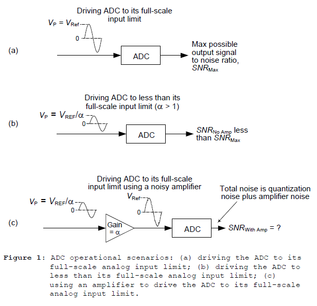
Here's the situation for an ADC whose maximum analog input voltage range is –VRef to +VRef. If we drive an ADC's analog input with an sine wave whose peak amplitude is VP = VRef, the ADC's output signal to noise ratio is maximized. We'll call that maximum signal to noise ratio SNRMax. That scenario is shown in Figure 1(a).
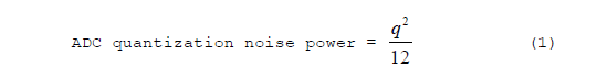
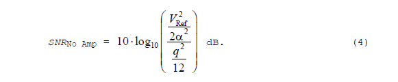
If, on the other hand, we drove an ADC's analog input with an sine wave whose peak amplitude is VP = VRef/α, where α > 1, the ADC's output signal to noise ratio will be less than SNRMax. That scenario is shown in Figure 1(b). In this case we're not driving the ADC to its full-scale analog input range and we'll call this output signal to noise ratio SNRNo Amp < SNRMax. Because we're not utilizing the full-scale analog input range of the ADC, we're losing potential ADC output signal to noise ratio.
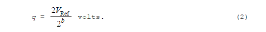
To overcome that loss of output signal to noise ratio in Figure 1(b) we can use an amplifier, with a voltage gain of α, to drive the ADC's input to fullscale as shown in Figure 1(c). We'll use the variable SNRWith Amp to represent the ADC output signal to noise ratio in this case. However, we must be cautious! Because we cannot buy an ideal noise-free amplifier at Radio Shack, we're forced to use an amplifier that has some non-zero output noise. In that case, the question becomes, "What is the maximum inherent amplifier noise we can tolerate and still ensure that SNRWith Amp > SNRNo Amp?" And the answer to that question is the point I'm attempting to make in this blog. Please read on.
ADC Quantization Noise
Just to remind you, the quantization noise power of an b-bit ADC, whose maximum analog input voltage range is –VRef to +VRef, is:
where q is the least significant bit (LSB) voltage range equal to
Equation (1) is based on the assumption that the ADC's input voltage crosses 4 or 5 LSB voltage boundaries, and is not synchronous with the ADC's sample frequency. The derivation of Eq. (1) is readily available on the Internet and in just about every DSP textbook.
ADC Output Signal to Noise Ratio
In the Figure 1(a) case, the ADC's output signal to noise ratio, in decibels, is:
In the Figure 1(b) case, the ADC's output signal to noise ratio is:
In the Figure 1(c) case, the ADC's output signal to noise ratio is:
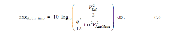
Because in Figure 1(c) we're driving the ADC to full-scale the numerator of the ratio in SNRWith Amp in Eq. (5) is equal to the numerator of the ratio in SNRMax in Eq. (3). The denominator of the ratio in Eq. (5) is ADC quantization noise power plus the amplifier's output noise power. The term VAmp Noise in Eq. (5) is the RMS of the amplifier's inherent internally-generated noise referred to the input of the amplifier. Thus the term α2 (VAmp Noise)2 is the amplifier's output noise power.
For a given ADC with an input signal that requires amplification by a gain of α, we want to know what is the maximum value of (VAmp Noise)2 so that SNRWith Amp is greater than SNRNo Amp? To answer that question we must compare Eqs. (4) and (5). We can make that comparison by first multiplying Eq. (4)'s numerator and denominator ratios by α2 giving us:

Now we can easily compare Eqs. (5) and (6) because they have identical numerator ratios. So all we have to do to make sure that SNRWith Amp is greater than SNRNo Amp is ensure that the denominator of Eq. (5) is less than the denominator of Eq. (6). That is, we want the following inequality to be satisfied:
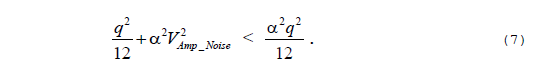
Rearranging Eq. (7), we want to ensure that the following inequality is satisfied:
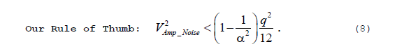
So there we have it. We want the amplifier's internally-generated noise power, referred to the input of the amplifier, to be a factor of (1-1/α2) less than the ADC's q2/12 quantization noise power.
It's instructive to plot the maximum (VAmp Noise)2 in percentage terms of the ADC's q2/12 quantization noise power, as a function of amplifier gain α. We do that in Figure 2.
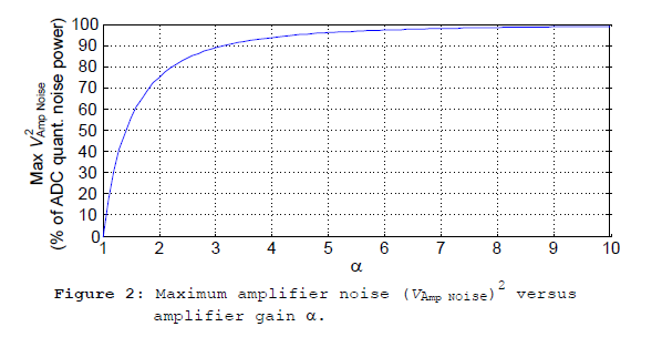
We interpret Figure 2 as follows: let's say our original analog input signal requires a voltage gain of α = 2 to drive an ADC to full-scale. For a value of α = 2, Figure 2 and Eq. (8) tell us that (VAmp Noise)2 must be no greater than 75% of the ADC's q2/12 quantization noise power.
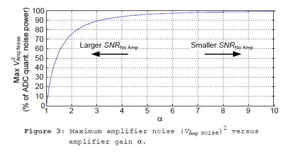
When I first looked at Figure 2 I noticed that it implied: for larger values of amplifier gain a larger values of (VAmp Noise)2 are acceptable. That means for larger values of a larger values of α2 (VAmp Noise)2 amplifier output noise power are tolerable. This didn't make sense to me until I realized: for larger values of gain a the value of SNRNo Amp will be smaller permitting larger acceptable maximum values for (VAmp Noise)2 as shown in Figure 3.
Conclusion
Given the specifications of an ADC and the necessary gain of an amplifier, Eq. (8) and Figure 2 tell us what must be the maximum amplifier output noise so that using an amplifier improves an ADC's output SNR relative to not using an amplifier. By the way, Reference [2] presents a useful tutorial on amplifier noise.

References
[1] This amplifier noise rule of thumb was taught to me by Prof. Ayman Fayed, ADC guru at Iowa State University.
[2] "Op Amp Noise", MT-047 Tutorial, http://www.analog.com/media/en/training-seminars/tutorials/MT-047.pdf


- Comments
- Write a Comment Select to add a comment
alpha > 1

It seems that the second half of you post failed to show up in your comment. I'm not sure what is the point you're trying to make. In any case, if alpha a <1 then we'd need an attenuator preceding the ADC, rather than an amplifier, to avoid overdriving the ADC.
[-Rick-]
i think abara meant that there is an error in you text: in your text ther is the sentence as abara has mentioned.It shall be "alpha>1"
Hello Rick,
Could you please update the second reference as it is currently not found.
Thanks!
Ibrahim
Hello Ibrahim. I believe that reference [2] is:
[2] "Op Amp Noise", MT-047 Tutorial, http://www.analog.com/media/en/training-seminars/tutorials/MT-047.pdf
To post reply to a comment, click on the 'reply' button attached to each comment. To post a new comment (not a reply to a comment) check out the 'Write a Comment' tab at the top of the comments.
Please login (on the right) if you already have an account on this platform.
Otherwise, please use this form to register (free) an join one of the largest online community for Electrical/Embedded/DSP/FPGA/ML engineers:


