


Which MOSFET topology?
A recent electronics.StackExchange question brings up a good topic for discussion. Let's say you have a power supply and a 2-wire load you want to be able to switch on and off from the power supply using a MOSFET. How do you choose which circuit topology to choose? You basically have four options, shown below:
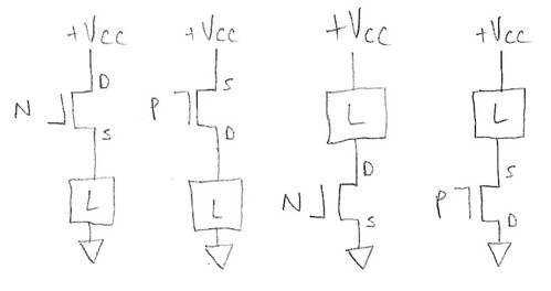
From left to right, these are:
- High-side switch, N-channel MOSFET
- High-side switch, P-channel MOSFET
- Low-side switch, N-channel MOSFET
- Low-side switch, P-channel MOSFET
Basically you can use an N-channel MOSFET or a P-channel MOSFET, and put the switch above the load or vice-versa.
A quick reminder about using MOSFETs: A MOSFET has 3 terminals, gate, drain, and source. I've illustrated drain and source with D and S, respectively; the other terminal is the gate. The MOSFET is controlled by the relative voltage Vgs between its gate terminal and its source terminal.
If Vgs = 0, the MOSFET is off and conducts essentially no current between its drain and source terminals (although there is parasitic leakage, usually specified as a maximum of 1-100uA). For an N-channel MOSFET, the current that flows between drain and source increases rapidly as Vgs increases above its gate-to-source threshold voltage Vgs(th); at some point the current that conducts is determined by the load resistance rather than the MOSFET, in which case the MOSFET behaves like a resistor between drain and source. The resistance depends on Vgs as well, and is specified in the data sheet for particular Vgs levels. Most MOSFETs are specified at either Vgs = 10V (for "regular" MOSFETS) or Vgs = 4.5V (for "logic-level" MOSFETS, so-called because they can be driven by a 5V logic power supply), although nowadays there are an increasing number of low-voltage MOSFETS that have resistance specified at 3.3, 2.5, or even 1.8Vgs.
The voltage between drain and source on an N-channel MOSFET must be positive, otherwise a parasitic body diode between drain and source conducts to keep the drain from being more than a voltage drop below the source.
There are other important parameters of MOSFETs that you need to be know about (parasitic gate-drain and gate-source capacitance), but let's forget those for now.
(A quick recap: Vgs determines the current that can potentially flow from drain to source. If that current can't flow because the load resistance is too high, then the MOSFET acts like a resistor rather than a current sink. There's a body diode that conducts if the drain is pulled below the source terminal)
For P-channel MOSFETs, the polarity is reversed. The source terminal is normally more positive than the drain, and the MOSFET is turned on by negative Vgs.
So back to our four topologies. The most common configurations are probably in this order:
3. Low-side switch, N-channel MOSFET (easiest/cheapest)
2. High-side switch, P-channel MOSFET
1. High-side switch, N-channel MOSFET
4. Low-side switch, P-channel MOSFET (you essentially never see this)
Why?
Well, let's think about it. MOSFETs are controlled by their gate voltage relative to the source terminal. Of the four topologies, the only one that is relative to circuit ground is the low-side N-channel switch. Driving this circuit is a piece of cake. You generate a voltage source of 0 volts to turn the MOSFET off, and 5 or 10V above ground to turn the MOSFET on. (See my earlier blog post, Byte and Switch, for some minor gotchas.)
To understand why you would use either topology #2 (high-side P-channel) or #1 (high-side N-channel), there are two very important things to consider:
Circuit ground
The word "ground" is often misused in electronics. What it's supposed to mean is a low-resistance connection to a reference voltage. If you have appliances at home with a metal chassis and a 3-prong plug, the chassis is connected to the 3rd prong, and when you plug it into the AC mains, it's connected to a metal post in your home that is sunk into the earth. (In a car, there's not a good conductive path to the earth, but the metal frame of the car is "ground"; in this and other applications that do not have a protective earth connection, the word "ground" is misleading and "return" is a better term.) This is done for two reasons: safety and electromagnetic interference (EMI).
The safety aspect is that the earth's ground potential is generally -- except in weird lightning storms -- a safe voltage, so you can touch a grounded metal chassis with your hand and stand on a floor and not worry about being electrocuted. Whereas if you stand on a floor and you touch an exposed piece of metal that is significantly different from earth ground, you are likely to get hurt. Different standards apply but the generally accepted threshold is in the 50-60V range.
The EMI aspect is that ground is a stable voltage potential, and if an appliance is packaged in a conductive chassis, the chassis acts as a shield to block both outgoing and incoming electromagnetic radiation. If you attach the chassis to another potential that wiggles up and down relative to ground, it acts as an antenna, and can both emit and receive unwanted electromagnetic radiation.
For both these reasons, there are many types of two-terminal electrical loads (pumps, fans, motors, heaters, etc.) where it works very well to connect one of the two terminals to circuit ground. If this is the case, we are forced to use a high-side switch, which rules out topologies #3 and #4.
Otherwise, there is almost no reason not to use the low-side N-channel MOSFET.
N-channel and P-channel MOSFETs are not created equal
The general rule of thumb is that for the same price or for a given die area (and price is proportional to the amount of silicon used, so these are well-correlated), you will get worse performance in a P-channel MOSFET than in an N-channel MOSFET. (The charge mobility in N-channel devices is better than P-channel devices; if you want to know more, you should ask someone else who knows more than I do about device physics.) On-resistance is a lot higher in P-channel MOSFETS. Furthermore, manufacturers generally offer more choices in N-channel devices, especially at voltages above 100V.
So, all other things being equal, you should use an N-channel MOSFET, because you have more device choices and higher performance for a given device cost.
So to recap: some applications require high-side switches because one terminal of the load needs to be tied to ground for safety/EMI reasons. And N-channel MOSFETs are cheaper than P-channel MOSFETs for the same performance specs. Got it?
If you need to use a high-side switch, you have a tradeoff to make: do you want the cheaper switch, or do you want the cheaper gate drive?
If you pick topology #1 (high-side N-channel MOSFET), the gate drive circuitry is a little tricky. You need to control Vgs, but the source voltage will get yanked up and down as the switch turns on and off, and when it's on, the gate voltage has to be 5-10V above the supply voltage Vcc. You either need an isolated power supply, or what's called a bootstrap power supply where the switch turning on/off runs a charge pump to transfer charge to a capacitor that rides up and down with the MOSFET source terminal. There are many integrated circuit high-side MOSFET drivers available, and if you're switching on and off rapidly (pulse-width modulation), this can work quite well.
If you pick topology #2 (high-side P-channel MOSFET), the gate drive circuitry is a little easier. To turn the MOSFET off, tie the gate to the supply voltage Vcc. To turn the MOSFET on, pull the gate 5-10V below the supply voltage Vcc. This is still harder to control than the low-side N-channel MOSFET, but it can be done. If the supply voltage is in the 5-15V range, then you can generally find a P-channel MOSFET so that you can just connect the gate voltage to either Vcc (MOSFET off) or circuit ground (MOSFET on).
The last topology, #4 (low-side P-channel MOSFET), uses the lower performance P-channel device and requires a tricky gate drive to be relative to the MOSFET source which varies as the switch turns on and off. You will essentially never see this used in practice -- there's no reason you shouldn't be able to use a low-side N-channel MOSFET instead to get the cost and complexity down.
So if the load doesn't need to be grounded, topology #3 (low-side N-channel) is the clear winner.
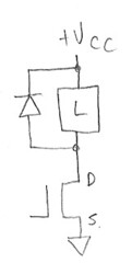
Finally, a reminder that we've skipped over an important detail that is missing from all 4 topologies shown. All loads, even a short length of wire, have some amount of inductance. A so-called "resistive" load like a heating element with a few feet of cable can still have a few microhenries of inductance. If you turn off the MOSFET, and you do not provide a path for the inductive current to flow, it will find its own path, by generating enough voltage to bring the MOSFET into breakdown conduction, and dissipate this energy in the MOSFET. Unless the inductance is small, you should use a freewheeling diode in parallel with the load to handle this current:
Happy switching!


- Comments
- Write a Comment Select to add a comment
I am using the IRF9321 P channel MOSFET for controlling my BLDC motor. The MOSFET is driven via a transistor which in turn is run by a freescale controller(3.3V pin). Now, when turning it on, it works fine. But, when turning it off its a disaster with the MOSFET taking almost 5ms to come to '0' Volts. I have been through the datasheet and it says turn off delay time is 180nSecs (approx .1uSecs).
Am I missing something? Also Sir, i have got no load.Its just to observe if the voltage comes out fine or not> I intend to connect a BLDC Motor to it. Will a load connected make it work better.
vinod
I am a student. Can you explain what " more than a voltage drop " means in this paragraph : "The voltage between drain and source on an N-channel MOSFET must be positive, otherwise a parasitic body diode between drain and source conducts to keep the drain from being more than a voltage drop below the source."
With other words, how would you say that?
Sorry for my english.

For the topology #1 (high-side N-channel MOSFET), I understand that the Source must be connected to the power supply, and the Drain to the load, so in that case the Source has a higher voltage than the Drain. If the body diode has a forward voltage threshold of 2 volts and you have a power supply of 20 volts, how do you switch off the MOSFET? Doesn't the current continue flowing through the diode?
I am assuming that a P-ch high side configuration would be the better bet, yes?
Thanks for any insight.
To post reply to a comment, click on the 'reply' button attached to each comment. To post a new comment (not a reply to a comment) check out the 'Write a Comment' tab at the top of the comments.
Please login (on the right) if you already have an account on this platform.
Otherwise, please use this form to register (free) an join one of the largest online community for Electrical/Embedded/DSP/FPGA/ML engineers:


