






REN9DB803DGLFT
Overview
The 9DB803DGLFT is a high-performance 8-output differential buffer designed specifically for PCIe Gen1 and Gen2 clock distribution. It functions as a zero-delay buffer or a fanout buffer to distribute high-speed HCSL clock signals across a system with minimal skew. The device operates from a 3.3V nominal supply and supports frequencies up to 400MHz.
Why Choose This Part
This buffer offers flexibility by allowing engineers to choose between PLL mode for zero propagation delay or bypass mode for standard fanout applications. With 8 HCSL output pairs and SMBus programmability, it reduces component count in complex systems while providing individual output control. The 5V tolerant I/O and wide 3.135V to 3.465V operating range ensure compatibility with standard digital logic levels.
Applications
Key Specifications
Getting Started
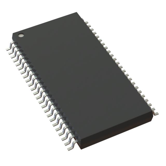
When designing with this part, ensure the SMBus interface is correctly pulled up to manage the output enable states and PLL configurations. Place the 48-TSSOP package near the clock source to minimize trace lengths of the HCSL input. Use a controlled-impedance 50-ohm or 100-ohm differential environment for all clock traces to maintain signal integrity at 400MHz.
9DB803 Family
Comparing specs that differ across variants. The current part is highlighted.
| Part Number | Package | Stock |
|---|---|---|
| 9DB803DGLFT (this part) | TFSOP-48 | 14,255 |
| 9DB803DFLF | BSSOP-48 | 630 |
| 9DB803DGLF (Renesas Electronics America/NEC) | TFSOP-48 | 188 |


