



EmbeddedRelated.com
BSC0502NSI

IFXBSC0502NSI

MPN: BSC0502NSIATMA1
Infineon Technologies
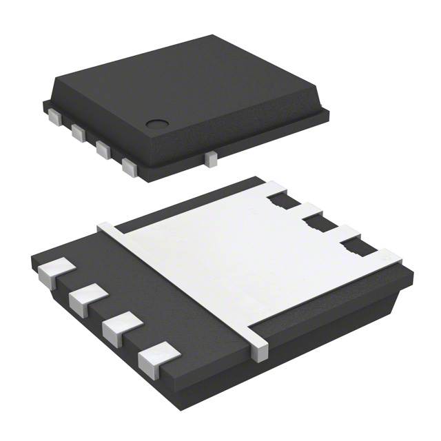
N-Channel 30 V 26A (Ta), 100A (Tc) 2.5W (Ta), 43W (Tc) Surface Mount PG-TDSON-8-6
Active32,664 in stock

Overview

The BSC0502NSI is a high-performance N-channel 30V MOSFET in a PG-TDSON-8 package, part of Infineon's OptiMOS range. It features a monolithically integrated Schottky-like diode to reduce switching losses and is specifically optimized for high-efficiency buck converters. With a maximum continuous drain current of 110A and an ultra-low RDS(on) of 2.3mOhm at 10V, it is designed for high power density applications.

Why Choose This Part

The integration of a Schottky-like diode significantly reduces the reverse recovery charge, which improves efficiency during the dead-time of switching cycles. Its low on-resistance and low gate charge (Qg) minimize both conduction and switching losses, while the 100% avalanche testing ensures robustness under inductive stress.

Applications

Synchronous Buck Converters
Optimized for the low-side switch position to minimize conduction and diode recovery losses.
CPU/GPU Power Delivery
Used in multi-phase VRMs for high-current processors in server and desktop environments.
DC-DC Point-of-Load Modules
Ideal for compact power modules requiring high efficiency in a small thermal footprint.
Battery Protection Circuits
Provides low-loss switching for high-current battery management systems in portable electronics.

Key Specifications

FET Type N-Channel
Vgs (Max) +/-20V
Technology MOSFET (Metal Oxide)
Mounting Type Surface Mount
Package / Case 8-PowerTDFN
Vgs(th) (Max) @ Id 2V @ 250uA
Operating Temperature -55degC ~ 150degC (TJ)
Rds On (Max) @ Id, Vgs 2.3mOhm @ 30A, 10V
Power Dissipation (Max) 2.5W (Ta), 43W (Tc)
Supplier Device Package PG-TDSON-8-6
Gate Charge (Qg) (Max) @ Vgs 26 nC @ 10 V
Drain to Source Voltage (Vdss) 30 V
Input Capacitance (Ciss) (Max) @ Vds 1600 pF @ 15 V
Drive Voltage (Max Rds On, Min Rds On) 4.5V, 10V
Current - Continuous Drain (Id) @ 25degC 26A (Ta), 100A (Tc)

Getting Started

When designing for high-current switching, minimize the gate-drive loop area and use wide PCB traces or copper planes for the drain and source connections to manage heat. Refer to Infineon's thermal simulation models to validate the PG-TDSON-8 cooling requirements under your specific load conditions.