





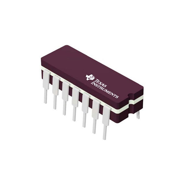
TICD4011BE
Overview
The CD4011BE is a CMOS quad 2-input NAND gate integrated circuit that operates across a wide supply voltage range from 3V to 18V. This device provides the system designer with direct implementation of the NAND function and features buffered inputs and outputs for improved noise immunity and drive characteristics. It is a fundamental building block in digital logic, notable for its extremely low power consumption of 0.01mA at 5V.
Why Choose This Part
The CD4011BE is highly versatile due to its ability to operate at high voltages up to 18V, making it much more robust against power supply fluctuations than 5V-only TTL logic. It features buffered outputs that provide symmetric source and sink current capability and high noise immunity, which is critical in industrial environments. The 14-PDIP through-hole package is ideal for prototyping and hand-soldering applications.
Applications
Key Specifications
Getting Started
To use the CD4011BE, connect VDD (Pin 14) to a positive supply between 3V and 18V and VSS (Pin 7) to ground. Ensure all unused inputs are tied to either VDD or VSS to prevent excessive quiescent current and noise. Because it is a CMOS device, use standard ESD precautions such as grounded wrist straps during handling and assembly.
CD4011 Family
Comparing specs that differ across variants. The current part is highlighted.
| Part Number | Package | Stock |
|---|---|---|
| CD4011BE (this part) | DIP-14 | 26,470 |
| CD4011BM96 | SOIC-14 | 41,260 |
| CD4011BEE4 | DIP-14 | 1,851 |


