





ONFDS4435BZ
Overview
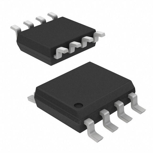
The FDS4435BZ is a 30V P-Channel MOSFET designed to provide low on-resistance and high power handling in a standard SO-8 footprint. Utilizing onsemi proprietary PowerTrench technology, it is optimized for high-efficiency power management and load switching applications. The device is rated for a continuous drain current of 8.8A and features a maximum RDS(on) of 20 mOhm at a 10V gate-source voltage.
Why Choose This Part
The FDS4435BZ offers a high ESD protection level and is designed to minimize switching losses. Its SO-8 package provides a familiar footprint for automated assembly while maintaining a low thermal resistance for a power dissipation rating up to 2.5W. The 25V maximum gate-source voltage rating provides a robust safety margin for 12V and 19V power rails.
Applications
Key Specifications
Getting Started
When designing with this MOSFET, ensure adequate copper pour area on the PCB at the drain pins (5-8) to act as a heatsink. Use a standard gate driver or a discrete transistor circuit capable of handling the gate charge for high-frequency switching. Verify that the gate-source voltage stays within the +/-25V limit during transient events.


