




EmbeddedRelated.com
Jacob Beningo
Live online course · Jacob Beningo
AI for Embedded Developers
$100 off for EmbeddedRelated readers until Dec 6 · 5 live sessions, Dec 7-11
Discount ends in
19days 02hrs 33min 12sec
Learn More →
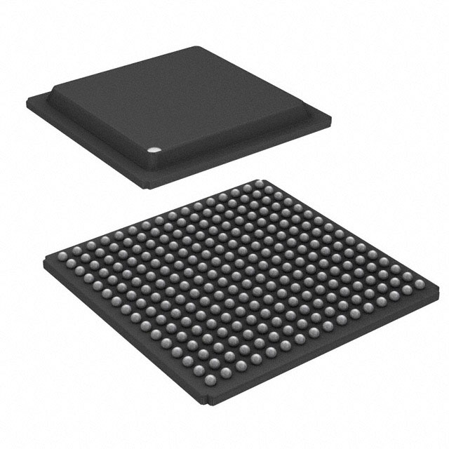
LFE3-35EA-6FTN256C

LFE3-35EA-6FTN256C

Lattice Semiconductor Corporation
ECP3 Field Programmable Gate Array (FPGA) IC 133 1358848 33000 256-BGA
Active179 in stock

Overview

The LFE3-35EA-6FTN256C is a mid-range LatticeECP3 Field Programmable Gate Array (FPGA) featuring 33,000 logic elements and over 1.3 Mbits of embedded RAM. Built on a low-power 1.2V process, it is designed for high-speed serial protocols and high-performance digital signal processing (DSP) applications. This device balances high I/O density with low power consumption in a compact 256-pin BGA footprint.

Why Choose This Part

This FPGA offers a high ratio of memory and DSP resources per logic cell, making it efficient for signal processing tasks. It includes advanced features like Soft Error Detect (SED) and TransFR I/O for simplified field updates and enhanced reliability in mission-critical environments.

Applications

High-Definition Video Processing
Utilizing integrated DSP blocks and high-speed memory for real-time video scaling, filtering, and color space conversion.
Industrial Networking Bridges
Implementing custom protocols for EtherCAT, Powerlink, or Profinet communication interfaces using pre-engineered source synchronous I/O.
Data Acquisition Systems
Managing high-speed data streams from ADC/DAC arrays with 133 I/O pins and flexible clocking via DLLs and PLLs.
Motor Control Inverters
Executing complex control algorithms for multi-axis robotics and industrial automation systems.

Key Specifications

Mounting Type Surface Mount
Number of I/O 133
Package / Case 256-BGA
Total RAM Bits 1358848
Voltage - Supply 1.14V ~ 1.26V
Number of LABs/CLBs 4125
Operating Temperature 0degC ~ 85degC (TJ)
Supplier Device Package 256-FTBGA (17x17)
Number of Logic Elements/Cells 33000

Getting Started

Designers should use Lattice Diamond software for synthesis, placement, and routing. Hardware debugging is supported through the Reveal Logic Analyzer and ORCAstra configuration utility via standard JTAG interfaces. Development often begins with the Lattice ECP3 Versa Development Kit to evaluate high-speed serial connectivity and logic performance.

Also Consider

Spartan-7 XC7S50 Xilinx (AMD) - An alternative high-performance 28nm FPGA for cost-sensitive applications requiring a modern toolchain and higher logic density.
ECP5 LFE5U-25F Lattice Semiconductor - The successor family providing improved power efficiency and higher-speed SERDES capabilities in a compatible package size.