




EmbeddedRelated.com
Jacob Beningo
Live online course · Jacob Beningo
AI for Embedded Developers
$100 off for EmbeddedRelated readers until Dec 6 · 5 live sessions, Dec 7-11
Discount ends in
19days 03hrs 05min 10sec
Learn More →
MX25U12832FZNI02

MX25U12832FZNI02

Macronix
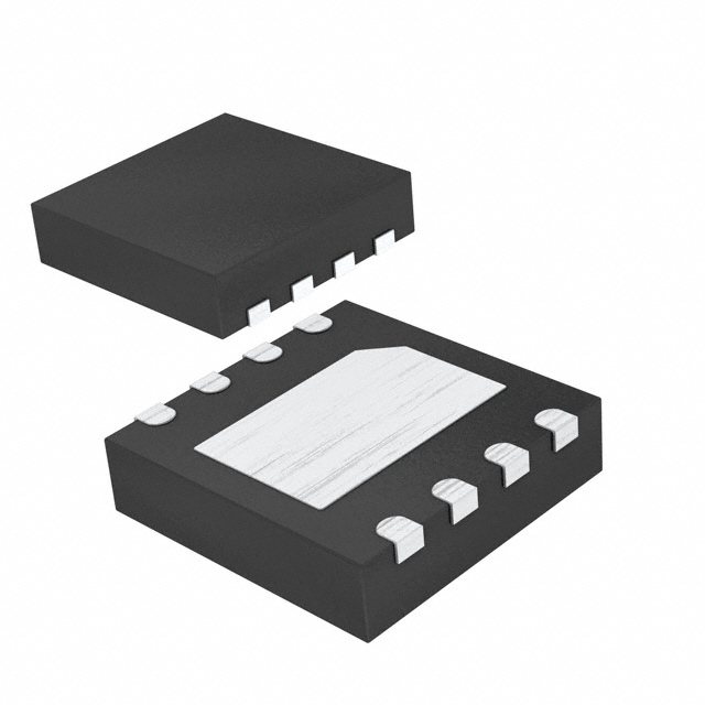
FLASH - NOR Memory IC 128Mbit SPI - Quad I/O, QPI 133 MHz 8-WSON (6x5)
Active2,070 in stock

Overview

The MX25U12832FZNI02 is a 128Mbit high-performance CMOS Serial NOR Flash memory operating on a low-voltage 1.8V rail. It supports Multi-I/O interfaces including Dual I/O, Quad I/O, and Quad Peripheral Interface (QPI) modes to achieve high data throughput up to 133 MHz. This device is designed for applications requiring fast boot times and high-density non-volatile storage in a compact 8-WSON package.

Why Choose This Part

This memory offers significant flexibility with its configurable dummy cycles and support for individual block erasing in 4K, 32K, or 64K byte segments. It features robust latch-up protection up to 100mA and includes Serial Flash Discoverable Parameters (SFDP) for easier software integration across different Flash vendors.

Applications

Execute-in-Place (XIP)
Utilizes Performance Enhance Mode and Quad I/O to run code directly from Flash, reducing the need for large internal RAM.
Industrial Controller Logging
Rated for J-grade temperatures up to 105C, making it suitable for storing logs and firmware in harsh industrial environments.
Low-Power IoT Edge Nodes
Deep Power-down mode with 15uA typical current and a 1.8V supply range makes it ideal for battery-operated wireless sensors.
High-Speed Boot Loading
The 133 MHz clock speed and 4xI/O read capability allow for rapid transfer of boot images to a system MCU or FPGA.

Key Specifications

Technology FLASH - NOR
Memory Size 128Mbit
Memory Type Non-Volatile
Memory Format FLASH
Mounting Type Surface Mount
Package / Case 8-WDFN Exposed Pad
Clock Frequency 133 MHz
Memory Interface SPI - Quad I/O, QPI
Voltage - Supply 1.65V ~ 2V
Memory Organization 16M x 8
Operating Temperature -40degC ~ 85degC (TA)
Supplier Device Package 8-WSON (6x5)
Write Cycle Time - Word, Page 40us, 3ms

Getting Started

When designing with this part, ensure your MCU or FPGA I/O bank is set to 1.8V as the device is not 3.3V tolerant. Implementation can be simplified by using standard SPI or QSPI peripheral libraries, and the 256-byte page buffer should be used to optimize programming throughput. Hardware designers should place a decoupling capacitor close to the VCC pin of the 8-WSON package to maintain signal integrity at 133 MHz.