





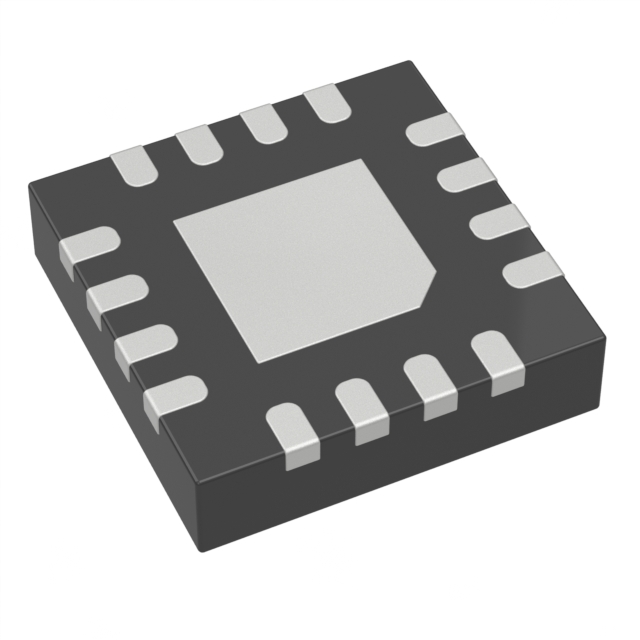
ONNB6L14SMNG
Overview
The NB6L14SMNG is a high-performance 1:4 differential fanout buffer and translator designed for high-frequency clock and data distribution. It supports input frequencies up to 2 GHz and provides four identical LVDS outputs with a typical supply voltage of 2.5V. Its flexible input stage accepts a wide range of signaling levels including CML, HCSL, LVDS, and LVPECL, making it an ideal interface for heterogeneous high-speed systems.
Why Choose This Part
This device offers a high 2 GHz bandwidth and integrated 50-ohm input termination resistors, simplifying PCB layout and reducing component count. The 16-VFQFN package features an exposed pad for improved thermal performance, while the wide input compatibility allows it to serve as a universal translator for multiple differential logic families.
Applications
Key Specifications
Getting Started
When designing with the NB6L14SMNG, ensure the exposed thermal pad is soldered to a ground plane to manage the maximum 100mA current draw effectively. Decouple the 2.375V to 2.625V supply with high-frequency ceramic capacitors placed as close as possible to the VDD pins. For optimal performance at GHz frequencies, use controlled-impedance transmission lines for all differential signal routing.


