





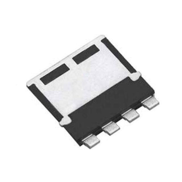
SQJQ100EL-T1_GE3
Overview
The SQJQ100EL-T1_GE3 is a high-performance N-Channel 40V TrenchFET power MOSFET housed in a PowerPAK 8 x 8L package. This AEC-Q101 qualified device is engineered for extreme current demands, supporting up to 200A continuous drain current and offering an ultra-low maximum RDS(on) of 1.2mOhm at 10V Vgs. Its robust construction allows for reliable operation in harsh environments with a maximum junction temperature of 175 degrees Celsius.
Why Choose This Part
The primary advantage is the exceptionally low 1.2mOhm on-resistance, which significantly reduces conduction losses in high-current paths. The PowerPAK 8 x 8 package provides superior thermal dissipation (150W max) compared to standard TO-220 or D2PAK footprints while maintaining a low profile. Furthermore, the AEC-Q101 qualification and 175 degrees Celsius rating ensure long-term reliability in demanding automotive and industrial thermal cycles.
Applications
Key Specifications
Getting Started
When integrating this MOSFET, prioritize PCB thermal management by utilizing multiple thermal vias under the PowerPAK drain pad to internal copper planes. Ensure the gate driver can source and sink sufficient peak current to manage the high gate charge for fast switching. Use high-power layout techniques, such as thick copper pours, to handle the 200A rated current without excessive trace heating.


