


Designing IoT Wireless Sensor Nodes
By Mahesh Balan
Wireless sensor nodes (WSN) play a fundamental role in enabling the Internet of Things (IoT). The strength of WSNs lies in the fact that they are extremely low powered, very small in size, and easy to install. For many IoT applications, such as those installed outdoors, WSNs can be powered using solar technology. While in the presence of light, the system is powered by the solar source, which also charges a tiny coin cell or super capacitor to power the system in the absence of light.
In general, wireless sensor nodes are sensor-based devices that monitor conditions such as temperature, humidity, or pressure. The node collects data from any kind of sensor and then wirelessly transmits this data to a control unit, such as a PC or a mobile device, where it is processed, evaluated, and acted upon. Ideally, nodes can operate as a standalone device by getting its operational power from an energy harvesting mechanism. In a general sense, energy harvesting is the process of capturing and converting tiny amounts of energy from sources like light, vibration, or heat into electricity.
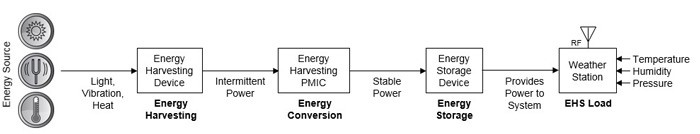
Figure 1: Energy Harvesting System Design Example
Figure 1 shows a block diagram of an energy harvesting system. Energy is collected by an energy harvesting device (e.g., solar cells) and converted to stable power using a power management IC (PMIC) which is then stored using low leakage, low-impedance capacitors. This power can then be provided to a sensor-interfacing load (e.g. MCU), which is used to transmit the sensor data wirelessly. In this diagram, the energy harvesting sensor (EHS) is the wireless sensor node.
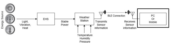
Figure 2: Wireless Sensor Node System Example
Figure 2 shows a block diagram for a wireless sensor node. Here, processed sensor data is transmitted wirelessly using Bluetooth Low Energy (BLE). BLE is the standard for short-range, low-power wireless applications that communicate state or control information. BLE operates in the 2.4-GHz ISM band with GFSK modulation and supports a 1 Mbps data rate.
The power management IC used to stabilize power from the energy harvesting device needs to support super-low-power operation itself. The PMIC S6AE103A from Cypress, for example, consumes only 280 nA and has a startup power of 1.2 μW (see Figure 3). As a result, even slight amounts of power generation can be obtained from compact solar cells under low-brightness environments of approximately 100 lx.
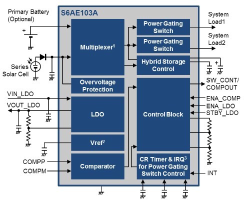
Figure 3: Block Diagram of S6AE103A PMIC for Energy Harvesting
Efficient Wireless Sensor Node Design
Let us now consider the various steps involved in the design of a WSN:
Step 1: Select the Hardware components
On the hardware side, you will need the appropriate sensors, an MCU that can be ultimately powered by the energy harvesting device, and a PMIC. There may also be additional passive components, depending on the design.
Sensors can be both analog and digital. Many of the sensors available today are digital sensors based on standard I2C, SPI or UART interfaces. Extremely low power sensors are also available. To keep device cost down and the form factor small, an MCU with integrated BLE can simplify design as well as reduce time-to-market. To further accelerate design, many vendors offer fully integrated, fully certified, programmable modules, such as the Cypress EZ-BLE Modules. Modules are complete with main MCU, two crystals, chip or trace antenna, shielding, and passive components. Because these modules already have the necessary BLE certifications, products can be released quickly into the market.
Figure 4: Example of BLE Module, the CYALKIT-E02 Solar-Powered BLE Sensor Beacon
Step 2: Design the Firmware and Estimate Power Consumption
With a programmable MCU selected, the next step is to write the appropriate firmware. The essential functions to be implemented in firmware are an interface to collect the sensor data, a BLE component or stack that can transmit the data wirelessly, and a CPU that can perform firmware processing.
Because super-low-power operation is critical, total current consumption needs to be considered from the start. Total current consumption is the sum of the current consumed by the sensors and the total current consumed by the MCU. Given that sensors typically do not consume much of the overall current, the focus should be to minimize the average current consumed by the MCU. Before optimizing the current, consider the three main components that will consume current in the MCU: the CPU, Sensor Interface Blocks (like I2C, SPI etc.), and BLE subsystem. Here, the major consumer of current will be the BLE radio while the radio is active (i.e., during BLE Tx and Rx).
Embedded MCUs offer various low power modes to reduce the current consumption. Firmware designer need to consider these low power modes and design code around them so that the average current consumption is minimized. For example, as sensor data does not change instantly, the firmware should scan sensor data only occasionally (for e.g., every 5 to 10 seconds, depending upon the sensor). The read data from sensors can be then transferred wirelessly over BLE.
As far the BLE firmware is concerned, sensor data can be sent along with the BLE advertisement packets. It is recommended not to send too much other overhead along with the advertisement packet as this can further increase the current. Between the advertising intervals and the sensor scanning intervals, the MCU should be put into low power modes like Deep-Sleep. A low power timer like a Watch-Dog Timer can wake up the device from Deep-Sleep once the timer count is expired. MCUs optimized for low power operation may offer a BLE internal timer that can wake up the device from Deep-Sleep after the advertisement interval has expired. Figure 5 shows the firmware flow to achieve this.
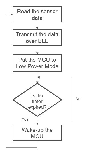
Figure 5: Firmware Flow for Efficient Wireless Sensor Node Design
Once the firmware is designed, you have to measure the current. You can use prototype boards for measuring the current. Note that the current needs to be measured separately for active and low power modes of the MCU. Once you know the time for which the MCU is in active and low power modes separately, the average current consumption would be:
(Iactive x Tactive) + (ILowPower x TLowPower)
Tactive+TLowPower
With this average current, you can find the average power by multiplying it with the PMIC voltage.
Step 3: Optimize the Firmware and Minimize the Average Current Consumption
It may be the case that the initial calculated power of the design is too high to be supported by the Solar PMIC. If this is so, you need to optimize the firmware. Here are effective ways to do this:
Optimize MCU Start-up code execution: While the MCU is starting up, you do not need high frequency external clocks like the 24MHz crystal generated clock for BLE operation. Disabling this clock initially will conserve energy. Also, watch crystals can take some time to stabilize, which is also usually part of the start-up. While these clocks are stabilizing, the MCU can again be put into low power mode and internal low frequency clocks can wake-up the device when the clocks are ready. In short, start-up code execution time can be significant and the firmware designer needs to minimize the start-up current consumed.
- Reduce the main CPU operating frequency
- Reduce the leakage current in pins used from the MCU by controlling their drive modes before entering low power modes
- Disable any debugging interface if the MCU supports it
These steps can help in reducing the average current consumption.
Step 4: Design the Hardware
With power-optimized firmware, it’s time to design the hardware based on the PMIC. Figure 6 shows a simple energy harvesting based PMIC design.
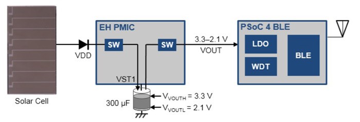
Figure 6: Simple Energy Harvesting Design
The PMIC first stores the solar energy in a storage device on VSTORE1 (VST1), which is a 300-μF ceramic capacitor in this example. When VST1 achieves VVOUTH, the energy is sent to the MCU. This simple energy harvesting design, however, cannot operate for the entire day as there is no backup capacitor. Let us now see how a backup capacitor can be added to the PMIC device and how it helps.
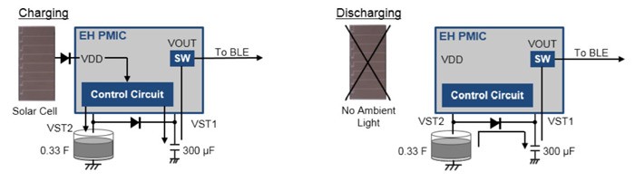
Figure 7: Energy Harvesting with Backup capacitor
The energy needed to operate the WSN is first stored in VST1 and the remaining energy is used to charge VST2. The energy stored in VST2 can be supplied to the WSN continuously when there is no ambient light. It is also possible to connect an additional coin-cell to the PMIC for much higher reliability as shown in Figure 8.
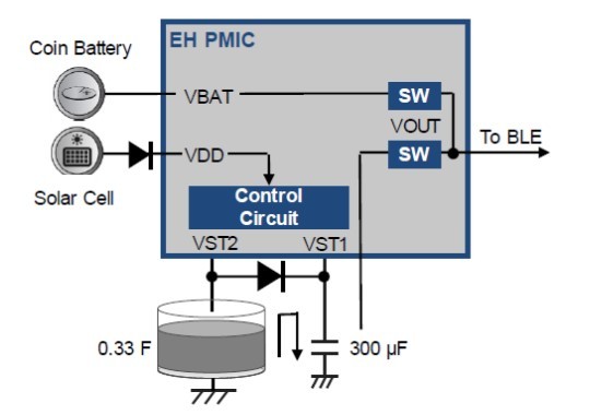
Figure 8: Energy Harvesting with Multiple Power Inputs
The PMIC converts both power sources so that WSN can operate in all conditions (even in the absence of light). The conversion happens automatically so that energy is supplied flawlessly to the WSN. So, this can be the optimal hardware design for the WSN.
Step 5: Design the User Interface
The user interface to a wireless sensor node can be as simple as a mobile application that can receive the data transmitted by the WSN. As the sensor data would be present at fixed positions of the advertisement packets, the BLE application can be designed to extract the relevant data from those positions and displayed on your phone. This technique can be used to manage more complex networks of multiple WSNs. For example, as shown in the following references:
References
EZ-BLE Module (Bluetooth Smart)
CYALKIT-E02 Solar-Powered BLE Sensor Beacon Reference Design Kit (RDK)
AN92584 - Designing for Low Power and Estimating Battery Life for BLE Applications
Author
Mahesh Balan earned his B.Tech in Electronics and Communication Engineering from Model Engineering College, India. He is currently working as a Staff Applications Engineer at Cypress Semiconductor on MCU based projects and assisting customers in their designs.


- Comments
- Write a Comment Select to add a comment
To post reply to a comment, click on the 'reply' button attached to each comment. To post a new comment (not a reply to a comment) check out the 'Write a Comment' tab at the top of the comments.
Please login (on the right) if you already have an account on this platform.
Otherwise, please use this form to register (free) an join one of the largest online community for Electrical/Embedded/DSP/FPGA/ML engineers:


