Hello!

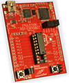
I just had a look at the manual to the motorola coldfire 5282 evb, and
I�d like to understand why they connected the sdram-chips to the
processor the way they did.

The schematics can be found at
http://e-www.motorola.com/files/soft_dev_tools/hardware_tools/printed_circuit_boards/M5282EVB-SCH.pdf

In short: They connected the chips to A9...A23. A0...A8 are not used by
sdram, but by the flash-rom, which ist connected as usual.

Any idea?

Tankred.

Weird memory design in M5282EVB
Started by ●February 10, 2004
Reply by ●February 10, 20042004-02-10
"Tankred M�ller" <tankred.mueller@epost.de> wrote in message news:c0as83$1503u8$1@ID-145595.news.uni-berlin.de...> Hello! > > I just had a look at the manual to the motorola coldfire 5282 evb, and > I�d like to understand why they connected the sdram-chips to the > processor the way they did. > > The schematics can be found at >http://e-www.motorola.com/files/soft_dev_tools/hardware_tools/printed_circuit_boards/M5282EVB-SCH.pdf> > In short: They connected the chips to A9...A23. A0...A8 are not used by > sdram, but by the flash-rom, which ist connected as usual. > > Any idea? > > Tankred. >My guess is that the chip has a built in SDRAM controller, and that is the configuration you need to wire it in for the controller to work correctly. DRAM is address by row and column, not by decoded address. Tony
Reply by ●February 10, 20042004-02-10
Yes, you are right!
I wasn�t aware that an internal memory controller doesn�t have to be
connected in the "normal" way.

Thanks for your help, today I got a bit smarter than yesterday...

Tankred.
Reply by ●February 10, 20042004-02-10
> I just had a look at the manual to the motorola coldfire 5282 evb, and > I�d like to understand why they connected the sdram-chips to the > processor the way they did.It's common on uCs that share (S)DRAM and flash/SRAM controller functions on a single address bus, to have the flash address pins count up from one "end" of the bus and the SDRAM address lines either to count down from the other "end" or just to be translated left some number of bits. I think the rationale is to cut down on the number of pin-state-changes in interleaved flash-SDRAM access cycles, in order to reduce EMI and perhaps improve performance in high-capacitative-loading situations. Since it's the LSbits that will be changing most frequently (on the flash controller anyway), it makes sense to separate those bits from the SDRAM control bits. Someone correct me please if this is grossly wrong and based on flawed science...


