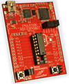
On Apr 17, 6:17 pm, Jim Granville <no.s...@designtools.maps.co.nz> wrote:> .. Probably because the software goal arrives in the form of some arm > waving from marketing! :):)> Since this is about hardware selection to match design goals, can you > add a CPLD footprint ?In an earlier incarnation I was going to use a high-end FPGA, but it's just too complex for my book. I'm already wondering how I'll get it finished in time and in roughly the page limit required.
Interest in AVR+MSP430 "general purpose" proto board?
Started by ●April 15, 2007
Reply by ●April 17, 20072007-04-17
Reply by ●April 17, 20072007-04-17
larwe wrote:> On Apr 17, 6:17 pm, Jim Granville <no.s...@designtools.maps.co.nz> > wrote: > > >>.. Probably because the software goal arrives in the form of some arm >>waving from marketing! :) > > > :) > > >>Since this is about hardware selection to match design goals, can you >>add a CPLD footprint ? > > > In an earlier incarnation I was going to use a high-end FPGA, but it's > just too complex for my book. I'm already wondering how I'll get it > finished in time and in roughly the page limit required.Yes FPGAs are complex things to learn, and the tools are large, and also a moving target. CPLDs are simpler, and a good stepping stone; the tools are stable, and relatively easy to learn and even easier to run. We have them setup to launch from a text editor, and single key compile/fit/simulate take 1-2 seconds. PGM is sub 10s. -jg
Reply by ●April 19, 20072007-04-19
larwe wrote:> - SD socket moved to overhang edge of board by ~80 mil in order to > protrude through edge of 1591ESBK box if desired.Is the back of this part of the board free, in case you want to mount the SD socket on the back, rotated 180 degrees, so the SD card doesn't overlap? Nice idea, BTW. Would be nice with a CPLD as Jim suggested.
Reply by ●April 19, 20072007-04-19
On Apr 19, 4:48 am, Clifford Heath <n...@spam.please.net> wrote:> > - SD socket moved to overhang edge of board by ~80 mil in order to > > protrude through edge of 1591ESBK box if desired. > > Is the back of this part of the board free, in case you want to > mount the SD socket on the back, rotated 180 degrees, so the SD > card doesn't overlap?There are currently no footprints at all on the back of the board, partly because for cost reasons I'm only putting silkscreen on the top side. That's a pretty good idea, though.> Nice idea, BTW. Would be nice with a CPLD as Jim suggested.All right, all right, what is with the CPLD? CPLD talk is not going to make it into my book, but just supposing I were to add it to this board, how would you want it wired? All the pins coming to headers, or half the I/Os going to a micro and the other half to a header?
Reply by ●April 19, 20072007-04-19
larwe wrote:> On Apr 19, 4:48 am, Clifford Heath <n...@spam.please.net> wrote: >>Nice idea, BTW. Would be nice with a CPLD as Jim suggested. > > > All right, all right, what is with the CPLD? CPLD talk is not going to > make it into my book, but just supposing I were to add it to this > board, how would you want it wired? All the pins coming to headers, or > half the I/Os going to a micro and the other half to a header?OK, here is one suggestion: Wire 4 CPLD pins to the uC(s), as SPI SPI_DI SPI_DO SPI_SS SPI_CK and some of the others can go to pin headers, - you can work out from their names, what they are used for, and some header candidates :) Pin Name Resource/Direction 43 on LCD_RWn Dge-- 44 on LCD_RS Dge-- 1 -- TDI INPUT 2 PT DB6 Dge-- 3 PT DB5 Dge-- 5 PT DB7 Dge-- 6 PT DB4 Dge-- 7 -- TMS INPUT 8 PT DB1 Dge-- 10 PT DB3 Dge-- 11 PT DB2 Dge-- 12 PT DB0 Dge-- 13 on LCD_E Tg-g- 14 -- SPI_DI INPUT 15 on SPI_DO C---- 32 -- TDO C---- 26 -- TCK INPUT 39 SPI_SS INPUT << Locked Pin 37 SPI_CK INPUT << Locked Pin Spares could go to backlight, and buttons - depends on board space really. and the programming pin header - IDC10 IDC10 CPLD pin --------+----------------------- JTAG.1 S PIN26_C62_TCK_B JTAG.2 S GND JTAG.3 S PIN32_C73_TDO JTAG.4 S VCCIO JTAG.5 S PIN7_C15_TMS_B JTAG.6 E PIN40_C90_GCLK2B JTAG.7 E PIN39_C89_GCLRB JTAG.8 E PIN37_C87_GCLK1B JTAG.9 S PIN1_C4_TDI_B JTAG.10 E GND_OR_VCCINT Jumper Selected. Allows JTAG unlock, Some PCBs GND.10
Reply by ●April 22, 20072007-04-22
larwe wrote:> While working on my next book, I've built a small general-purpose > prototyping board. This PCB is also intended to be useful for thoseOkay - I'm running a bit behind schedule, but not much; I'll be ordering boards this week, just not Monday. An updated schematic and component layout are posted at <http://www.larwe.com/zws/products/ polyceph/index.html> - this will be the permanent home for the project. I think I've incorporated everything except the CPLD; no room to fanout those I/Os on a 2-layer board [at least not with my mediocre routing skills].


