


Introduction to PIC Timers
Continuing getting started with PIC 8-bit development, this fourth in a series of five articles looks at configuring and using timers on the PIC 8-bit platform. Topics discussed include:
- PIC Timers
- Timer0 Module
- Timer Application
The completed code for this post can be downloaded from GitHub.
PIC®, MPLAB® X, PICkit™ 4 On-Board, and PICkit™ 4 are trademarks of Microchip Technology Inc.
mikroBUS™ is a registered trademark of MikroElektronika.
All data sheet references are to Microchip document
PIC18F27_47Q10-data-sheet-40002043C, © 2019 - Microchip Technology
Inc, available
here
at the time this post was published.
Background
The initial post in the series reviewed Microchip’s development hardware offerings and the available Microchip development tools and used MPLAB X Code Configurator (MCC) to generate a simple application to light an LED. The second post focused on basic PIC 8-bit memory organization, including the role of GPRs (General Purpose Registers) and SFRs (Special Function Registers), explored oscillator and clock configuration for processor start up, refining the initial configuration to meet application requirements, and wrapped up walking through the oscillator / clock start up and configuration code generated by MPLAB X’s MCC tool. The third post looked at 8-bit GPIO and developed a simple application, still with the assistance of MCC, to flash a series of four LEDs.
All posts thus far have relied on MPLAB X's MCC for configuring and generating at least part of the application. For hardware, a PIC18F47Q10 40 pin PDIP package was used on a breadboard with a PICkit 4 debugger / programmer. For this post, hardware switches to the Curiosity HPC Development Board with the same PIC18F47Q10 processor. The Curiosity HPC Development Board includes an integrated debugger / programmer, the PICkit 4 On-Board (PKOB4), a selectable 3.3v / 5v power source, and various external components (switches, potentiometer) including 4 LEDs configured as active high tied to the PIC18F47Q10 Port A upper nibble. Also available on the board but not utilized for this application are two mikroBUS connectors. This post also uses MPLAB X IDE (version 6.20) but not MCC.
PIC Timers
The processor datasheet refers to the peripheral as a timer, specifically a Timerx module. From previous posts the ‘x’ suffix is a common datasheet approach denoting generically a specific port or module of which a particular processor has multiple instances. The datasheet also frequently uses the term counter in conjunction with the timers. In other literature, Microchip uses the terminology Timer/Counter referring to the peripheral. Regardless of how they are referenced, timers and counters are go to workhorse peripherals for many tasks.
Basic Timer behavior can be broadly captured by four
characteristics:
- Measures a programmable period
- Has a clock with configurable input sources
- Counts inputs from the timer’s clock source
- Performs an action when the clock input count reaches the
period, referred to as a match
The datasheet shows three types of timer modules, Timer0 and Timer1, and Timer2. Each module provides a slightly different implementation of the four characteristics listed above. The source of input counter varies by timer module and can be the processor clock, the internal high frequency oscillator, a signal source external to the processor, etc. When using the processor clock or internal oscillator, the peripheral acts timer like, as the processor clock period is a known value. The timer’s configured period is therefore a multiple of that clock period resulting in a match occurring after a known time interval. When the input source is external to the processor, the peripheral acts more like a counter. Perhaps the external inputs being counted are from a rotary encoder measuring the rotation of a motor shaft; in this case the timer period would be set to the desired number of revolutions for the motor. The size of the period varies by module; for the PIC18F47Q10, the various modules provide for 8-bit and 16-bit values, some timer modules can be configured for either with slightly different behavior for each. Going back to the example of using the timer to measure an interval of elapsed time using the processor clock, longer intervals can be specific using 16-bit values. Later in this article, pre- and post- scalers are examined to help better manage the need for counting larger number of input counts than can be captured with just an 8-bit or 16-bit period values. Finally the action performed when the actual count reaches the target value is customizable by timer module. Possible actions include but are not limited to setting an SFR bit value, triggering a processor interrupt (interrupts are covered in depth in the next post), toggling a value on a GPIO pin, resetting the current count thereby enabling continual operation, or some possible combination thereof.
A discussion of all the available timer modules and their various modes and behaviors is a topic too broad for an introduction to timers. The requirements for the application associated with this post is a timer that can toggle an SFR bit every second. The application monitors that bit to toggle the state of four external LEDs. This application uses Timer0 as it is a basic timer implementation without some of the mode complex and diverse configuration and operational capabilities as the Timer1 and Timer2 modules. As such, it serves as a good vehicle for understanding basic timer configuration and operation.
Timer0 Module
The datasheet section 18. Timer0 Module provides the necessary architecture, description and register documentation for the module. The basic implementation of the module is captured in the datasheet's Figure 18-1. Timer0 Block Diagram:
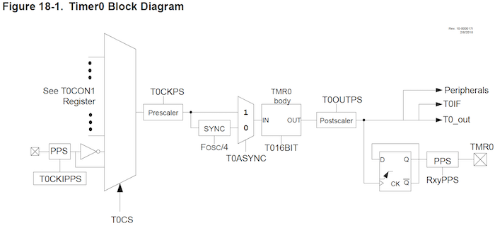
Operation Mode
The Timer0 module can operate in 8-bit or
16-bit mode. The operation mode determines the size of timer
period. There are two Timer0 SFRs dedicated to the period
and count elements of the timer: TMR0H, TMR0L. When Timer0
is configured as an 8-bit timer, TMR0H holds the timer period
while TMR0L holds the timer count. When configured as a
16-bit timer, both the TMR0H, TMR0L registers are configured as a
16-bit counter for the timer. In 16-bit operation there is
no means to set a period, instead Timer0 acts as a free running
timer. When the counter reaches the maximum value of 0xFFFF,
the counter rolls over to 0x0000 and continues counting up.
Clock Source
The module’s clock source provides the input signals the timer
counts. The Timer0 clock can be
driven by a number of sources, including:
- CLC1_out (Configurable Logic Cell)
- Various Internal Oscillators
- Processor Clock / 4
- Various processor pins
Consider an application configuring the processor clock to run at a speed of 8MHz. When operating in 8-bit mode, with a clock source of the Processor Clock / 4, the maximum period the timer could measure is:
$$ {\pmb F _{Timer\,Clock}} = {{F_{osc}} \over 4} = {8000000\,Hz \over 4} = {2000000\,Hz} $$
$$ {\pmb T} = {1 \over frequency} = {1 \over 2000000\,Hz} = {0. 0000005\,sec} $$
$$ {Max\,Period = 256 * 500\,nS = 128\,uSec} $$
Pre-scaler
The Timer0 module provides a pre-scaler to extend the period the timer can measure. A pre-scaler sits between the timer clock source and the timer clock input. The pre-scaler acts as an input source divider; for every n clock inputs, the pre-scaler outputs one clock signal to the timer’s counter register. As it effectively slows down the clock source, the pre-scaler can significantly increase the measurable period of the timer. For Timer0 the pre-scaler can range from 1:1 (no clock source division) to 1:32768. Continuing with the above example using a processor speed of 8MHZ and a timer clock source of Fosc / 4, operating in 8-bit mode with a prescaler rate of 1024, the maximum time interval increases to:
$$ {\pmb F _{Timer\,Clock}} = {{F_{osc}} \over 4} = {8000000\,Hz \over 4} = {2000000\,Hz} $$
$$ Prescaler = {2000000\,HZ \over 1024} = {1953.125\,Hz} $$
$$ {\pmb T} = {1 \over frequency} = {1 \over 1953.125\,Hz} = {0.000512\,sec} $$
$$ {Max\,Time\,Interval = 256 * 0. 000512 = 131.072\,mSec} $$
Following similar calculations, with the same parameters except operating in 16-bit mode the maximum time interval is 33.55 seconds.
A tradeoff of using a pre-scaler value is that while a larger time interval can be measured, the resolution is significantly decreased. The effect is linear – the larger the pre-scaler the more coarse the resolution. With the above examples, using a timer clock of Fosc/4 with FOsc = 8MHz, with no pre-scaler, the time interval has a resolution of 500nSec. The same configuration with a pre-scaler of 1:16384 has a resolution of 819.2 uSec.
Postscaler
In addition to prescaler functionality, the Timer0 module has post-scaler capabilities. Like the pres-caler, the post-scaler acts as a divider for the clock output. With a post-scaler of 1:1, the clock outputs a signal for each timer match. Applying a larger post-scaler value, 1:n, holds the timer output by n matches. As with the pre-scaler, the post-scaler has a similar drawback in that the available resolution of the timer interval is reduced with larger post-scaler values.
Actions
In 8-bit mode, when the Timer0 counter value matches the period, the count is reset and a bit, T0OUT, in the control register T0CON0 is toggled signaling the match event. When configured as a 16-bit timer, both the TMR0H, TMR0L registers are configured as a 16-bit timer/counter. When the 16-bit counter overflows, that is reaches 0xFFFF, the same T0OUT in the control register T0CON0 is toggled; the timer counter rolls over to 0x0000 and continues counting. The Timer0 overflow bit, TMR0IF is also set in the PIR0 register. This flag can be used to trigger a processor interrupt. Interrupts are looked at in the last post of this getting started series.
Registers
The datasheet documents four SFRs associated with Timer0 module; two 8-bit registers dealing with operation, two 8-bit registers for peripheral configuration.
T0CON0
T0CON0 is the first configuration / control SFR. The configuration elements of the register are used to select the previously discussed 8-bit or 16-bit operating mode and selecting the output post-scaler value. The control functionality of the SFR consists of enabling / disabling the timer module and the timer output bit, T0OUT. The datasheet calls out that the behavior of T0OUT differs between 8-bit and 16-bit timer modes. In the 8-bit mode T0OUT toggles on a match, in 16-bit mode T0OUT toggles on overflow.
T0CON1
T0CON1 is also a Timer0 module configuration register. The three configuration elements this register controls are the clock source selection, timer synchronization with the system clock (Fosc/4) and selecting a pre-scaler value.
TMR0H
TMRH0 is one of the operating registers. When operating in 8-bit mode, TMR0H holds the period value for the timer. When operating in 16-bit mode, TMR0H holds the upper 8 bits of the 16-bit counter.
TMR0L
TMRL0 is the other operating register. When the timer is operating in 8-bit mode, TMR0L holds the current count value for the timer. When operating in 16-bit mode, TMR0L holds the lower 8 bits of the 16-bit counter.
Timer Application
The application utilizes Timer0 configured with a one second period driving the toggle of the same four external LEDs used in the previous GPIO post. The application is configured to use the internal high frequency oscillator to drive the processor clock at a frequency of 8Mhz. The application is developed using MPLAB X version 6.20 and utilizes the Curiosity HPC Development Board with an 8-bit PIC18F47Q10 .
Timer Configuration
The application uses the Timer0 module in 8-bit mode. The timer’s clock source usea the processor clock divided by four. Earlier calculations showed that operating the timer in 8-bit mode with a time clock source of Fosc / 4, the longest duration the timer can measure is 128 uSec. Clearly, the application needs to use a pre-scaler, a post-scaler or a combination of both to achieve a period as close to one second as possible. A spreadsheet calculating the range of periods available using a timer clock speed of 2MHz with pre-scaler of 1:16384 and 1:32768 is available in the source control repository linked in the introduction of this article. As the two selected pre-scalers are multiples, the same period appears for both with simply different values for TMR0H. From the spreadsheet, the closest the application can get to the required one second period with a 1:16384 pre-scaler is 0.999424 seconds using a value of 121 in TMR0H.
Project Creation
As some of the project creation screens appear a bit different between the previously used v6.0 of MPLAB X and v6.2 used here, screen captures of the project creation assistant are shared here.
Open MPLAB X and select New Project from the File menu…

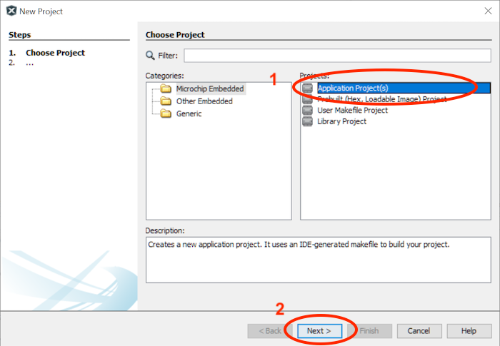
From the New Project assistant, Microchip Embedded folder, select Application Project(s) and click Next.
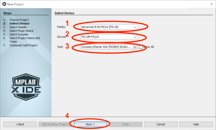
In the next New Project assistant step, select the Family from the drop down that filters the Device list (you can optionally simply start typing in the Device dropdown) and then the Tool from the available drop downs. Note that the selected tool, in this case the Curiosity HPC Board, needs to be connected to the workstation and recognized by MPLAB for the tool to appear in the drop down. If using the Curiosity HPC Board the Device Selection should appear as below. Click Next:
Next select the Compiler and click Next:

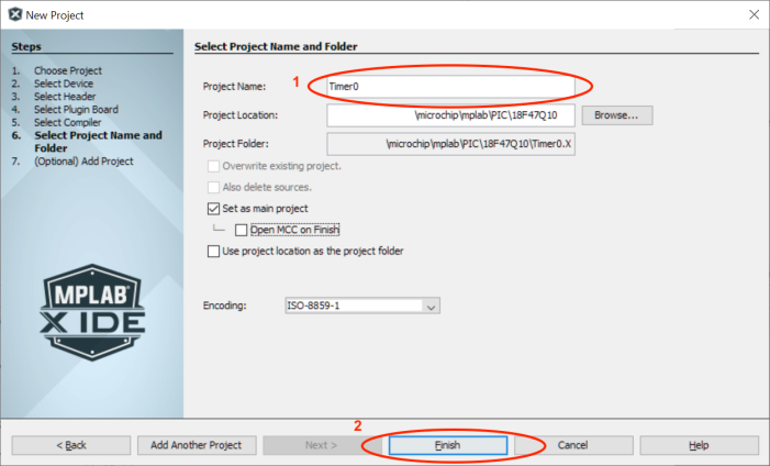
The final step needed to create the project is to name the project, select a save location and click Finish.
IMPORTANT
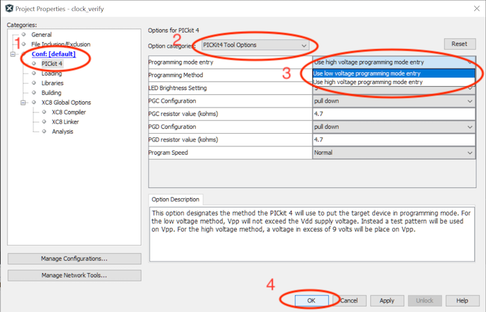
The next step is extremely important to not cause processor damage. Low Voltage Programming Mode Entry must be selected for the project regardless of the tool selected.
Failure to do so could result in damage to the processor.
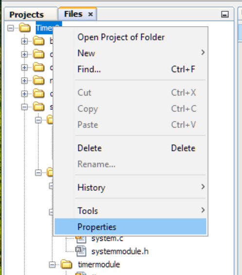
Right click on the project and select Properties from the menu:

Within Project Properties, select the Config: PICkit 4 category, then select PICKit4 Tool Options from the Option Category drop down and finally, select Use low voltage programming mode entry in the Programming mode entry drop down. When your settings appear as below, click OK.
Project Structure
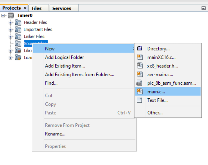
At this point MPLAB X has created an empty project. The next logical step is to get a basic project structure in place, but first a main.c source file needs to be added. MPLAB X can help by creating a file that has the proper header file include structure for the selected processor. Right click on the Source Files virtual directory, click New and then main.c:
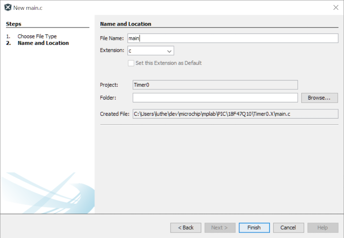
In the resulting dialog change the name to main. Folder
can remain blank, as the file will be created in the project
director as shown in the
Created File text box.
MPLAB X adds a new file with an include for the system level xc.h header. Please see the second post in this series for details on the structure of the xc.h header file.
#include <xc.h>
void main(void) {
    return;
}
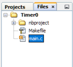
MPLAB X adds new files created in the IDE into the main project directory by default. The IDE implements a Logical Folders concept within the Projects window to provide project structure. This can be confirmed by looking at the Files window, which is a view of the physical project structure on the disk. From the Projects window, the just added main.c source file appears in the Source Files Logical Folder while the Files window shows the file in the root physical project folder, that is there is no physical Source Files folder in the project’s directory structure:

|
|
The Logical Folder structure is an MPLAB X concept. If porting the project to another IDE, unless that IDE has an understanding of MPLAB X project structure, will simply import the source files into a flat structure. To make the file structure more IDE agnostic, this post takes the approach of creating a physical file structure then mapping that file structure into the Logic Folder construct presented by the Projects window within the MPLAB X IDE. This approach of mapping an on-disk hierarchy to the MPLAB X Logical Folder structure is completely optional; if the project is solely managed within MPLAB X, the approach of adding files to a Logic Folder structure which maps into a flat physical directory structure is all that is needed. An added benefit of creating a physical directory structure is that the Files windows can also be used to manage the project as easily as the Projects window.
Physical File Structure
There are numerous schemes for managing folder structures in an embedded project. This post takes the approach of creating modules for each block of discrete functionality. For this application, there are three defined modules:
- System
- GPIO
- Timer
Each module has one or more source files, a header file with “top level” declarations consumed by the main application or other modules, and an optional header file declaring functionality used exclusively by the module.
Additionally, there is a single folder for all module header files that are included in the main application and/or other modules. This single folder collecting all the header files simplifies configuring the compiler Include directories property by providing a single directory containing all module header within the project.
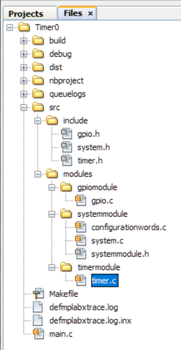
The physical folder structure for the project appears under the src folder as:

Application Modules
System Module
The System module is responsible for managing the ConfigurationWords via compiler directives as well as configuring the oscillator and processor clock related SFRs. The second post in this series discusses the ConfigurationWords as well as the SFRs to manage the oscillator and processor clock. Additionally, this module also initializes the five processor ports to known (default) values. The third post of this series discusses port initialization.
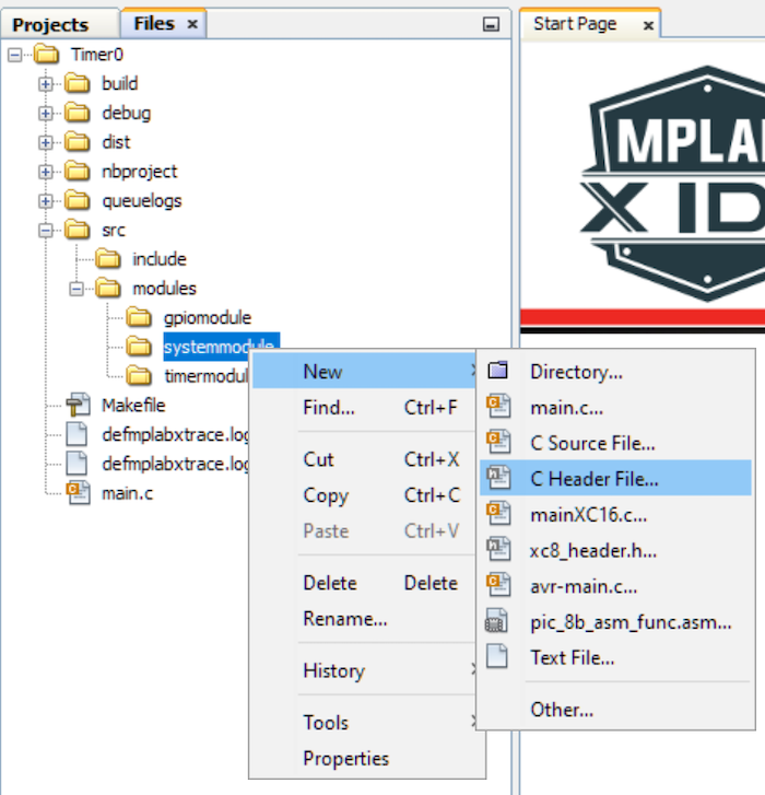
The system module consists of two source files, system.c and configurationwords.c both in the systemmodule folder and two header files, system.h residing in the include folder and systemmodule.h residing the systemmodule folder . Two empty source files can be added through the IDE. From the Files window, right click on the target parent folder, select New and then C Source File…
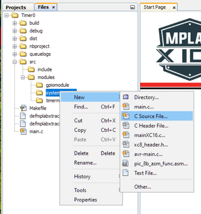
The header files can be similarly added through the IDE; from the Files window, right click on the target parent folder and select New and then C Header File…
Once the files are added the folder / file structure appears as:
The system.h header file (in the include folder) declares the function for initializing the system:
#ifndef SYSTEM_H
#define    SYSTEM_H
#include <xc.h>
void initializeSystem(void);
#endif    /* SYSTEM_H */
The systemmodule.h header file (in the systemmodule folder) imports the system.h header file as well as declares the module level functions needed for initialization.
#ifndef SYSTEMMODULE_H
#define    SYSTEMMODULE_H
#include "system.h"
void systemConfigureClock(void);
void systemConfigurePORTs(void);
#endif    /* SYSTEMMODULE_H */
The configurationwords.c source file contains the compiler directives for writing the configuration words.
The system.c source file contains the implementation for the three configuration functions declared in in system.h and systemmodule.h headers.
GPIO Module
The GPIO module is responsible for configuring and mapping the four GPIO outputs to the external LEDs, connected to the upper nibble of port A: RA7 (pin 13), RA6 (pin 14), RA5 (pin 7) and RA4 (pin 6).The module has a “top level” header file residing in the include folder, gpio.h. The source file, gpio.c, resides in the gpiomodule folder.

The include file, gpio.h, provides a definition for the initialization of the four pins of port A:
#ifndef GPIO_H
#define    GPIO_H
#include <xc.h>
void configureGPIO(void);
#endif    /* GPIO_H */
The gpio.c source file provides the implementation of the GPIO initialization function. This initialization code is discussed in the third post of this series.
Timer Module
The Timer module is responsible for configuring the timer used in the application as well as providing a means to start the timer.
The include file, timer0.h, provides a definition for the initialization and starting of Timer0:
#ifndef TIMER0_H
#define    TIMER0_H
#include <xc.h>
void configureTimer0(void);
void startTimer0(void);
#endif    /* TIMER0_H */</xc.h>
The timer.c source file provides the implementation of the related Timer0 functions:
#include "timer.h"
void configureTimer0(void) {
    T0CON0 = 0;
    T0CON1 = ( (0b010 << _T0CON1_T0CS_POSITION)
             | (0b1110 << _T0CON1_T0CKPS_POSITION) );
    TMR0H = 121;
}
void startTimer0(void) {
    T0CON0bits.T0EN = 0b1;
}
Setting the T0CON0 register performs the following configuration:
- Clears the T0EN (Timer0 ENable) bit (bit 7) – disables the timer
- Clears the T016BIT bit (bit 4) – configures the timer for 8-bit operation
- Configures T0OUTPS (Timer0 OUTput PostScaler) bits (bit3
3:0) – selects 1:1 postscaler
Setting the T0CON1 register performs the following configuration:
- Clears the T0CS (Timer0 Clock Select) bits (bits 7:5) - selects Fosc/4 as timer source
- Clears the T0ASYNC (Timer0 ASYNChronous) bit (bit 4) – synchronizes the timer input with Fosc/4
- Configures T0CKPS (Timer0 ClocK PreScaler) bits (bit3 3:0) – selects 1:16384 prescaler
Setting TMR0H to 121 configures the timer to generate a match every 0.999424 seconds.
Main Application
With the necessary initialization, configuration, and management functions in place, the next step is to set up the main application. The main.c source file pulls in the necessary headers, performs initialization, monitors the timer for a match, and when a match is detected, toggle the state of the external LEDs.
#include "system.h"
#include "timer.h"
#include "gpio.h"
void main(void) {
    initializeSystem();
    configureGPIO();
    configureTimer0();
    startTimer0();
    int currentT0OutputState = 0;
    while(1) {
        if(currentT0OutputState != T0CON0bits.T0OUT) {
             LATA ^= 0xF0;
             currentT0OutputState ^= 1;
        }
    }
    return;
}
The implementation starts with the one-time functions to initialize the system and configures the four GPIO output values as well Timer0.
When there is a Timer0 match, the T0OUT bit in the T0CON0 register toggles. In order to determine when that toggle happens, the current value of the T0OUT needs to be tracked; this is accomplished via the currentT0OutputState variable.
Within the while loop, the value of the T0OUT bit is continuously polled until a change occurs. Upon detecting the change, the new state of the T0OUT bit is saved, the LEDs are toggled and polling continues.
Project Updates
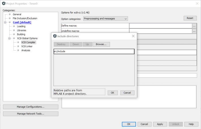
With the code in place, the compiler configuration needs to be updated by adding the new src/include folder to the Include directories list. The compiler configuration is accessed by right clicking on the Project (in either the Files or Project window) and clicking Properties.
From the Project Properties window, click the XC8 Compiler entry under XC8 Global Options. Add the src/include folder in the Include directories text box.
The physical folder and file structure can be easily mapped to the Logic Folder structure in the project tab which also ensures the source files are compiled as part of the project. Right click on Headers Files and click Add Existing Item...
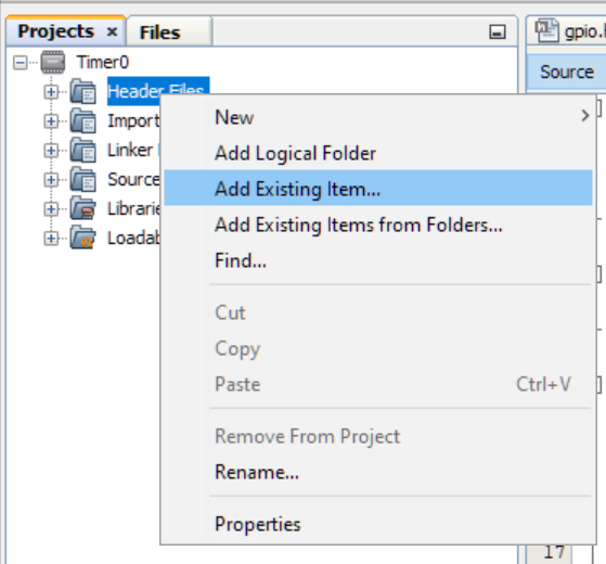
In the resulting window, navigate to src/include folder and select the three header files.
The modules folders can be mapped by right clicking on the project and clicking Add Existing Items From Folders….
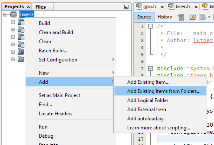
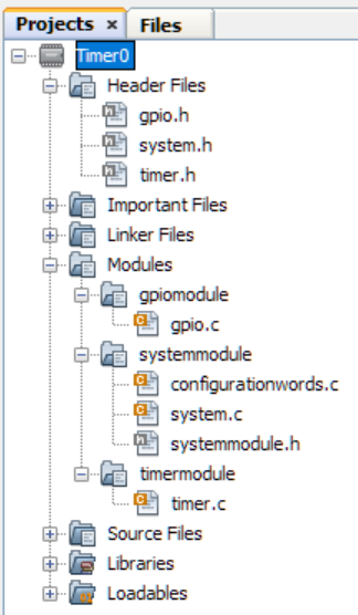
In the resulting window navigate to and select the src/modules folder. Add Existing Items from Folders... only pulls in source files; the systemmodule.h header file will also need to be explicitly added. Once everything is added, the Projects window should appear as:
The project can now be built, uploaded to the process and
run. With successful programming the LEDs will begin to
blink.
Verification
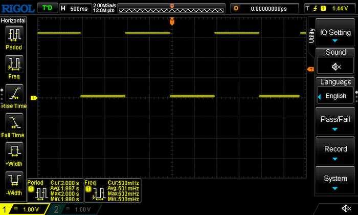
Verifying the expected period of flashing can be accomplished with an oscilloscope connected to any of the LEDs.
Final Thoughts
While slightly more efficient than the approach of a processor delay function taken in the third post, there is still a need to actively poll the T0OUT bit to determine when to toggle the LEDs. Other tasks can be completed by the processor between each poll, however, depending on the timing and duration of those tasks, the expected two second blink period could be off; in the case of a very long running task between polls, a complete toggle could be missed. The current two second period is also long compared to the processor clock speed. For timing tasks with much shorter periods closer to the processor speed, the possibility of variable periods or completely missing a period become more likely. The last post in this series looks at how interrupts can provide a means to allow the processor to complete other tasks with the program flow being interrupted when a timer match occurs.
Summary
Starting with a quick general overview of 8-bit PIC hardware timers, Timer0 elements such as Operating Mode (8-bit / 16-bit), Clock Source, Pre- and Post-Scalers and Match Actions were reviewed; many of these concepts are applicable to other timer modules such as Timer1 and Timer2. Finally, an application was put together to flash the four familiar LEDs. While developing the application a slight detour provided a better understanding of how MPLAB X can be used to manage a physical file structure and map that structure into logical project structures.


- Comments
- Write a Comment Select to add a comment
To post reply to a comment, click on the 'reply' button attached to each comment. To post a new comment (not a reply to a comment) check out the 'Write a Comment' tab at the top of the comments.
Please login (on the right) if you already have an account on this platform.
Otherwise, please use this form to register (free) an join one of the largest online community for Electrical/Embedded/DSP/FPGA/ML engineers:


