Getting Started With CUDA C on an Nvidia Jetson: GPU Architecture
Overview
In the previous blog post (Getting Started With CUDA C on Jetson Nvidia: Hello CUDA World!) I showed how to develop applications targeted at a GPU on a Nvidia Jetson Nano. As we observed in that blog post, performing a calculation on a 1-D array on a GPU had no performance benefit compared to a traditional CPU implementation, even on an array with many elements. In this blog post, we will learn about the GPU architecture to better explain the behavior and to understand the applications where a GPU shines (hint: it has to do with graphics). A better grasp of the GPU architecture will help us understand why GPUs are ideally suited for AI. In the next blog post, we will implement a representative algorithm to see the speed-ups achieved using a GPU.
CPUs vs GPUs
Traditionally, microprocessors based on a single CPU "core" (i.e., compute element) drove rapid performance increases and application cost reductions. Performance has been the driving factor when developing newer CPU technologies. Specifically, CPU developers have aimed to provide more functionality and features to users. There was a cycle in this development where the main focus of improvement was the clock rate.
However, starting from around 2003, the reduction in the size of computational devices (such as laptops, and then the introduction of smartphones and tablets) has shifted the focus from pure power to energy consumption and heat; these two metrics have been driven by extending the battery life of such devices. This has resulted in a focus shift for processor vendors from clock rate to the number of cores in a processor. This hardware design change has resulted in a fundamental difference in software development.
Software development has traditionally been focused on sequential operations. Software developers have relied on hardware advancements to improve software speed. However, when hardware development shifted to multiple compute elements, software development moved to a different paradigm. The emphasis was placed on developing applications that performed more operations in parallel.
There were two main trajectories for microprocessor development:
- Multicore: This class of processors aims to maintain the execution speed of sequential applications but increase the number of cores in a computing element. For example, consumer-grade Intel/AMD CPUs can have up to 16 cores. Each core is an out-of-order, multiple-instruction processor executing the complete x64 instruction set. Hyperthreading (Multithreading in AMD processors) effectively doubles the number of cores (from a software perspective).
- Manycore: This class of processors focuses more on the execution throughput of parallel applications than each compute element's speed. Each generation sees a multiple increase in the number of cores. For example, the Nvidia P100, one of the first GPUs introduced to the market, executed many simple, in-order instructions. Compared to their CPU counterparts, Manycore processors have traditionally been designed to optimize floating-point operations (i.e. FLOPS). The focus has been on calculation throughput.
The focus on the calculation throughput of GPUs has resulted in fundamental design differences. As mentioned, CPU design has been optimized for sequential code performance. This resulted in a design that uses sophisticated control logic to allow instructions from a single thread to execute in parallel or even non-sequential order while maintaining the appearance of sequential execution. The goal of CPUs has been to keep instruction and data access latencies to a minimum by having large cache memories. This design decision is motivated by ensuring that a user's experience of an application is not hindered by hardware latencies. For example, a CPU contains control logic for branch prediction to allow the CPU to predict a possible code path before it is decided.
CPU design has also been driven by memory bandwidth. Due to the asymmetry of CPU and memory speed, where memory speed has generally lagged CPU speed, application speed has been dictated by the data transfer rate from system memory to the CPU.
GPUs' focus on gaming has resulted in an architecture focused on calculating throughput and transferring large am data to and from system memory. GPU architecture focuses less on control logic and cache and more on compute elements.
Summary
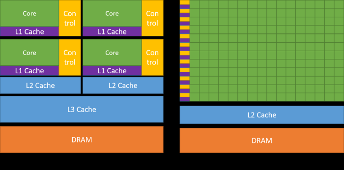
Based on the above summary of the motivation behind the design of CPU and GPU architectures, the following image shows the general architectural differences between CPUs and GPUs:

The CPU architecture on the left devotes a fair bit of silicon to control logic and different typesou ntof caches. Again, this has been driven by the desire to reduce memory accesses by the CPU. Additionally, each compute element (i.e. "Core") is larger and can support more complex operations. On the right, which shows the layout of the GPU silicon, we see that more area is devoted to a large number of smaller compute elements. Again, this is because the motivation of the GPU, founded in gaming, is to perform many simple floating-point operations on a set of pixels. In the next blog post, we will see how we can observe the architectural differences in implementing an algorithm meant for the GPU. We will see why our 1D implementation didn't result in these improvements, but a 2D will definitely result in improvements.
- Comments
- Write a Comment Select to add a comment
To post reply to a comment, click on the 'reply' button attached to each comment. To post a new comment (not a reply to a comment) check out the 'Write a Comment' tab at the top of the comments.
Please login (on the right) if you already have an account on this platform.
Otherwise, please use this form to register (free) an join one of the largest online community for Electrical/Embedded/DSP/FPGA/ML engineers:


