


Getting Started with the Microchip PIC® Microcontroller
Welcome to the first of five posts focusing on getting started with Microchip's 8-bit PIC® microcontrollers. The series of posts introduce successive topics culminating in a final project implementing a simple 4-bit counter with a "UI" of four external LEDs connected to GPIO pins counting up at a one second interval via an internal timer.
This post introduces the Microchip 8-bit PIC® Processor family:
- Overview of the various PIC® 8-bit families
- Reviewing Development Board Options
- Installing the MPLAB® X Integrated Development Environment
- Breadboarding with the PIC18F47Q10 using a MPLAB® PICkit™ 4 In-Circuit Debugger
- Configuring the PIC18F47Q10 via MCC (MPLAB® Code Configurator)
- Validating the selected PIC18F47Q10 configuration through clock output and LED
Subsequent posts cover the following topics:
Part II - Understanding Microchip PIC® 8-bit Family Configuration
Part III - Working with Microchip PIC® 8-bit Family GPIOs
Part IV - Working with Microchip PIC® 8-bit Family Timers
Part V - Working with Microchip PIC® 8-bit Family Interrupts
What is a PIC® Microcontroller
PIC® is a group of microcontrollers manufactured by Microchip. According to Microchip, PIC® is an acronym for Peripheral Interface Controller. The microcontroller was originally developed by General Instruments as a 16-bit core to handle input / output tasks for larger CPU chips. The current PIC® offerings are broad, with 8, 16, and 32-bit processors available.
Within the 8-bit offerings, where this posts focuses, are four families: Baseline, Mid-Range, Enhanced Mid-Range, and High-End. All families are based on a Harvard architecture / RISC instruction set with an 8-bit wide data bus. The family designation defines capabilities such as available memory, pin count, power requirements, available peripherals, etc. The PIC® part number identifies the processor family, again from Microchip (https://microchipdeveloper.com/xwiki/bin/view/products/mcu-mpu/8bit-pic/) the family part number map appears as:
| Family | Part Number |
|---|---|
| Baseline | 10Fxxx, 12Fxxx, 16Fxxx |
| Mid-Range | 10Fxxx, 12Fxxx, 16Fxxx |
| Enhanced Mid-Range | 12F1xxx, 16F1xxx |
| High-End | 18Fxxxx, 18FxxJxx, and 18FxxKxx |
The series of posts focuses on the High-End PIC18F47Q10.
Hardware: Getting Started
Microchip makes getting started developing for any of the PIC® 8-bit families easy. Three options are readily available ranging from lower cost with less flexibility to higher cost with maximum flexibility - there are always tradeoffs in anything we do as engineers!.
Option 1: Curiosity Development Board
Microchip has two rich offerings for 8 bit development. The first, DM164137, supports lower pin count devices: 8, 14, and 20 pin devices. The second, DM164136 focuses on higher pin count devices: 28 and 40 pin devices. Both offer sockets allowing the board to work with a wide range of processors. Both boards ship with an 8-bit processor; the DM164136 includes a PIC16F18446 while the DM164136 includes a PIC18F47Q10. These development boards deliver a lot of functionality out of the box at a modest price. In addition to being able to easily use different processors, each board comes with various external peripherals such as switches, LEDs, and / or potentiometers, etc. as well as a version of Microchip’s PICKit™ programmer/debugger. At least one MikroElectronika Mikrobus™ interface populates the boards allowing seamless use of any of the numerous Click Boards™ available from MikroElectronika. Finally, these boards include standard female headers making every pin of the processor available enabling easy connection of the processor with external circuits, breadboards, etc. With a micro-USB cable and an installation of MPLAB® IDE you can be running and debugging code in minutes without needing to purchase any additional tools.
Option 2: Curiosity Nano Development Platform
A second option from Microchip is the Curiosity Nano series of development boards. Much smaller in size than the aforementioned Curiosity Development boards, the Nano boards typically focus on smaller pin count devices supporting only a single processor soldered on the board. The Nano Curiosity boards do include an integrated programmer / debugger, many also include limited peripherals for testing and experimentation – typically one or two LEDs and perhaps a push button switch. Microchip does offer an expansion base for connectivity between Nano boards and mikroBus™ Click Boards® - part number AC164162. Like the development boards, the Nano Curiosity boards typically expose most if not all processor pins via standard spaced 0.1” (2.54mm) solder pads on the board. Male headers (included with most of the Nano boards) can be added to use the Curiosity Nano with a breadboard either via male – female jumpers or inserting the Nano directly into the breadboard. The pads on the Nano board are slightly offset such that the male headers can be held in place with a friction fit not even requiring soldering! While a nice feature, I always prefer the solid electrical connection afforded by soldering the headers to the board . As there are few pins available, the lower pin count devices may run into limitations of using multiple on-processor peripherals concurrently with general IO pin functionality. If the goal is developing a solution for a single PIC® processor and there is a Nano board available, this solution can be the most cost-effective.
Option 3: Discrete Processors
Most of the 8-bit family of PIC® processors are available in PDIP packaging and therefore breadboard compatible. Besides the ability to select any available processor for development, the options for peripherals are limitless. As an industry we are fortunate to enjoy ready access to not only discrete components such as LEDs, switches, resistors and transistors but also external I2C / SPI peripherals from manufacturers such as SparkFun, AdaFruit, etc. – ranging from humidity sensors, various LCD and OLED displays, GPS, Flash / sRAM memory, and serial to USB converter to name a few. This option also requires a MPLAB® PICkit™ 4 for programming / debugging and a suitable power supply; most of the 8-bit PIC® processors can be powered from via the common 3.3v or 5v ranges. Lastly, a breadboard and a selection of jumper wires will be needed.
Options Summary
Discrete Processors |
|
| Benefit |
Limitation |
|---|---|
| Unlimited Peripheral Options | Longer set up |
| Widest Processor Selection |
Highest Initial Cost |
| Support for Additional Process Families | |
Curiosity Development Boards |
|
| Benefit |
Limitation |
| Wide Peripheral Selection via mikroBUS™
Socket(s)
|
Processor Selection Limited by Pin Count |
| True "Out of the Box" Ready Solution |
Mid-level Initial Costs |
Curiosity Nano Development Boards |
|
| Benefit |
Limitation |
| Lowest Initial Cost |
No Ability to Easily Swap Proccesors |
| Limited Peripheral Options w/o Additional
Purchases
|
|
| Limited to Mostly Lower Pin Count Devices |
|
PIC18F47Q10 Processor
This series of posts starts with a discrete processor / breadboard option and transitions to a High Pin Count Curiosity Development board to give a feel for the different approaches. The same processor, the PIC18F47Q10 is used throughout and pin selection is made to ensure compatibility with the GPIO peripherals, primarily LEDs, on the Curiosity Development board. Other processors can certainly be used, as similarity between the various processors is an attractive feature of the PIC® line, however, the data sheets for both the processor and the chosen development board / option will need to be consulted for both on-processor peripheral settings and well as GPIO port selection / mapping.
The datasheet for the PIC18F47Q10 shows a processor with 128KB of flash (program) memory, 3728 bytes of SRAM and 1KB of EEPROM. The processor also includes on-chip peripherals including (2) I2C/SPI modules, (2) Extended USART modules, (3) 8 bit timers, (4) 16 bit timers as well as support for the PIC® Peripheral Pin Select functionality.
Without further delay – let’s get the processor wired up on a bread board and get an LED lit!
Hardware: Wiring Up a Solution
Background
The first project routes the processor clock to the OSC2 / CLKOUT pin - Port A, bit 6 (RA6). From the datasheet RA6 maps to pin 14 on the 40-pin PDIP package. Exposing the clock signal as part of an initial solution allows verification of the clock configuration (the same configuration, once verified, is used in subsequent posts) with an oscilloscope.
The project also lights a low current LED connected to Port A, bit 4 (RA4); pin 6 on the 40-pin PDIP package. Port RA4 was specifically selected as it is also connected to an LED on the HPC Curiosity Development Board in the event you selected that option instead of the discrete processor / breadboard option. Also note that this circuit defines RA4 as active high – that is the LED lights when RA4 is configured as an output GPIO and is toggled high, again in line with the behavior of the HPC Curiosity Development Board. GPIO port detail and implementation are covered in a subsequent post.
MPLAB® PICkit™ 4 In-Circuit Debugger
Programming is accomplished with the MPLAB® PICkit™ 4 In-Circuit Debugger (note the MPLAB® PICkit™ 5 is now available). The MPLAB® PICkit™ 4 User's Guide recommends a 10-50KΩ pull up resistor on the VPP/MCLR pin.
The user guide for the MPLAB® PICkit™ 4 documents eight female pins, referred to as the ICSP SIP, on the end of the programmer opposite the end with the Micro-B USB connector. One end of the ICSP SIP is denoted with a small black triangle, Pin 1 of the connector. The functions of the various connections of the ICSP connector:
| Pin | Function |
|---|---|
| 1 | VPP/MCLR |
| 2 | VDD |
| 3 | VSS |
| 4 |
PGD (Program Data) |
| 5 |
PGC (Program Clock) |
| 6 |
Not Used for ICSP |
| 7 |
Not Used for ICSP |
| 8 |
Not Used for ICSP |
Other Elements
For this project, the 40pin PDIP PIC18F47Q10 is powered by a 3.3V source. This voltage source also determine the value of the LED current limiting resistor. The LED in use is a low voltage / current LED - part# HLMP-1719 or equivalent.
Schematic
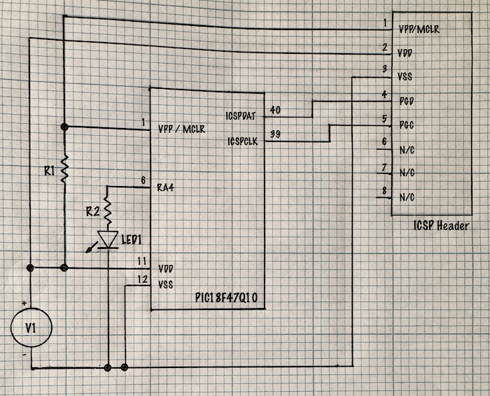
Bill of Materials
- R1 - 47KΩ
- R2 - 1KΩ
- LED1 - HLMP-1719 or equivalent
- V1 - 3.3V source
Power Up
With wiring and connections completed and double-checked, power up the circuit with the 3.3V power source and connect the MPLAB® PICkit™ 4 to a USB port on the development computer.
Software
NOTE: Version 6.00 of the MPLAB® X Integrated Development Environment and MCC plugin version 5.4.11 were used to develop the application. The screenshots that follow were taken from the Windows version of those tools. While the flow should be similar across versions, some specific screen details or options may appear different in newer versions of the IDE and the associated plugins and processor packs.
Install the IDE
MPLAB® X is Microchip’s Integrated Development Environment (IDE) for working with almost any of the PIC® microcontrollers. The IDE is cross platform with support for Windows, Linux and macOS. Download the appropriate package for your platform from the Microchip website and check any installation notes in the download area. Launch the downloaded installer and follow the prompts. Also be sure to download and install the 8-bit compiler as this is a separate download / install from the IDE.
Create the Project
Open MPLAB® X and after installing any recommended updates / packs, select New Project from the File menu...
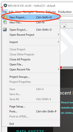
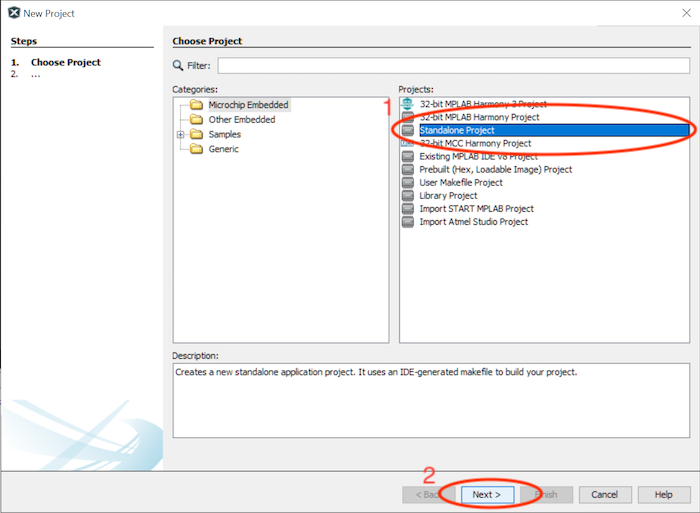
From the New Project wizard Choose Project step, select Stand Alone Project and click Next.
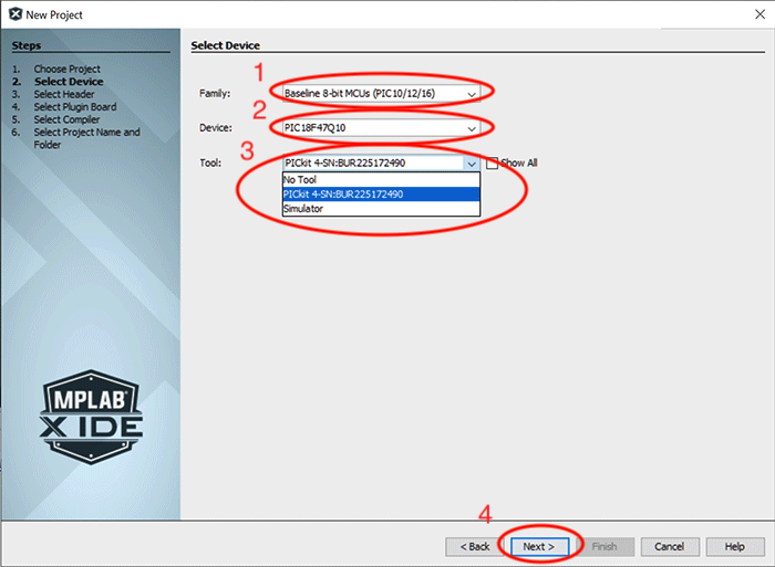
In the next New Project wizard step, select the Family from the drop down that filters the Device list (you can optionally simply start typing in the Device dropdown) and then the Tool from the available drop downs. Note that you will need to have the selected tool, in this case the the PICkit™ 4, connected to the workstation and recognized by MPLAB® for the tool to appear in the drop down. If using the PICkit™ 4, when your screen matches the capture below, click Next:
Next select the Compiler and click Next: 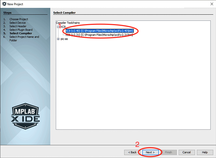
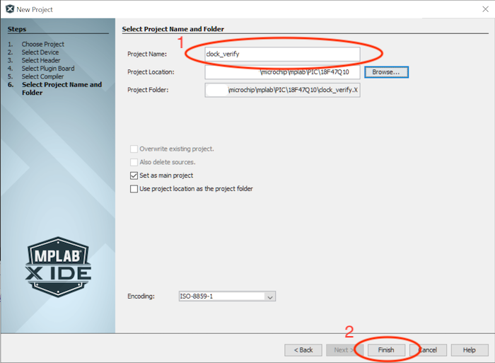
And lastly, at least for the New Project wizard, enter a Project Name and Project Location then click Finish.
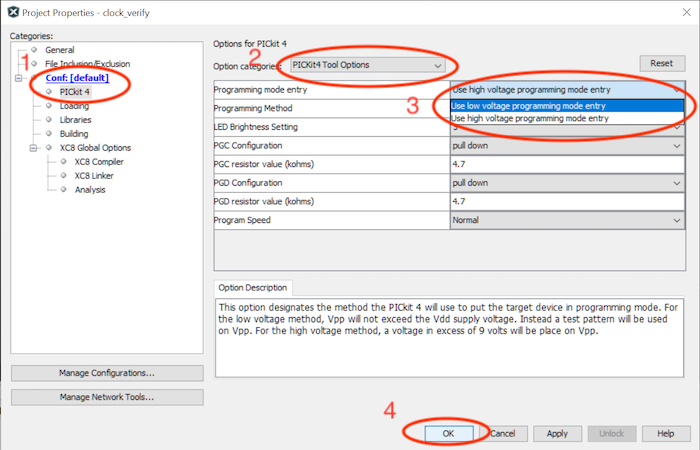
IMPORTANT
The next step is extremely important to not cause processor damage. Low Voltage Programming Mode Entry must be selected for the project regardless of the tool selected.
Failure to do so could result in damage to the processor.
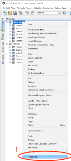
Right click on the project and select Properties from the menu:
Within Project Properties, select the Config: PICkit 4 category, then select PICKit4 Tool Options from the Option Category drop down and finally, select Use low voltage programming mode entry in the Programming mode entry drop down. When your settings appear as below, click OK (or Apply then OK).
Processor Configuration
MPLAB® X provides a means to graphically configure various processor settings and peripherals used in the project through the MCC (MPLAB® Code Configurator) tool. While this is a convenient means to set up items such as Configuration Registers, Pin Assignments, GPIO Pins, enable / configure peripherals (USART, SPI, I2C) it obfuscates the detail of the inner workings of the processor. While this works well for some projects, without a fundamental understanding of what / how / why of the configuration the engineer can be at a significant disadvantage when troubleshooting or when advanced setup is required. I prefer to directly program to the registers, while that may not be for everyone I do strongly encourage everyone to take the register approach at least once to better understand the available tools. With that in mind, outside of setting up basic one-time processor configuration (such as clock sources and clock dividers) I do not normally use MCC for configuration. In this post, as we are simply lighting up an LED and not discussing GPIO in depth, I do use MCC to alleviate the need to write any code to configure a GPIO pin. Subsequent posts cover in depth the GPIO configuration we are relying on MCC to provide here.
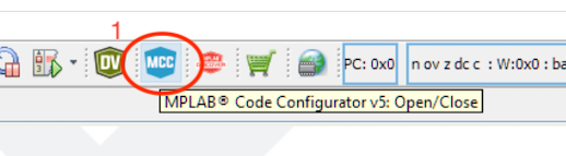
MCC is launched through a button on the IDE toolbar.
When MCC opens, the MCC Content Type must be selected. Select MCC Classic; the following flow and screenshots are from MCC Classic.
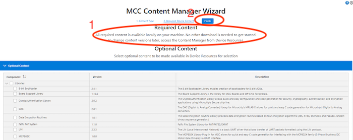
After the Content Type is selected, a wizard launches to select Required Content and Optional Content. If this is the first time MCC is run, there may be some Required Content which needs to be downloaded and installed. Once you get to the screen below showing all Required Content is available, click Finish.
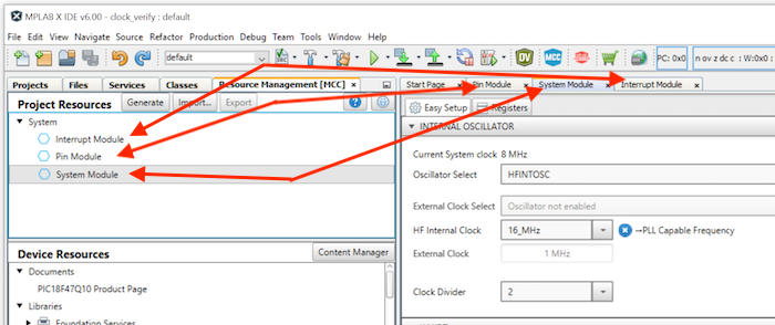
Once MCC is launched, the Resource Management (MCC) tab opens in the left pane containing three modules corresponding to the three windows opened in the editor pane: Pin Module, System Module, and Interrupt Module. Two modules – the System Module and the Pin Module are used in this project - the former for oscillator and clock configuration, the latter for GPIO configuration.
Select the System Module editor; there are two sub-tabs – Easy Setup and Registers. While the actual how and why of this module is covered in a subsequent post, this post simply enumerates the step by step process to get our processor configured to expose the system clock on a processor pin. From Easy Setup, configure the INTERNAL OSCILLATOR as below:
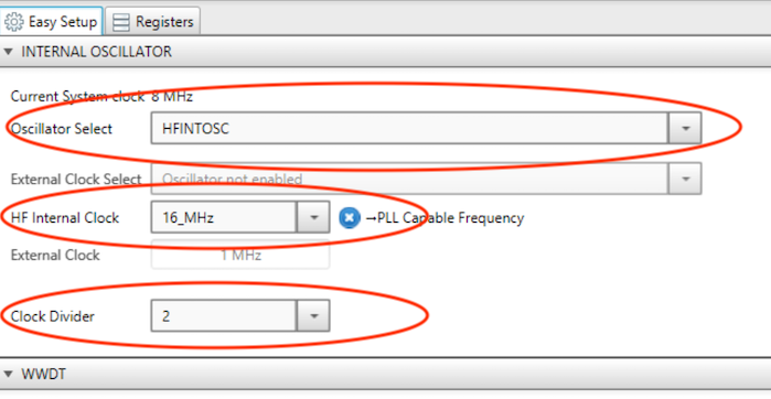
Oscillator Select – HFINTOSC
This sets the processor oscillator source to the High Frequency INTernal OSCillator
HF Internal Clock – 16_MHz
This sets the internal oscillator speed to 16MHz
Clock Divider – 2
This determines the divider value for the HFINTOSC which then becomes the System Clock. Note that the Current System clock in the tab updates reflecting the selected configuration.
The remaining values (such as those in the WWDT section) should be left at default.
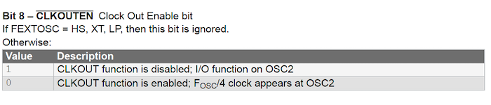
There is no Easy Setup option for routing the clock signal to an external processor pin (RA6 for the PIC18F47Q10). This functionality is enabled via the MCC Register sub-tab in the System Module tab in the editor pane. The setting to change appears in the Register: CONFIG1H section.
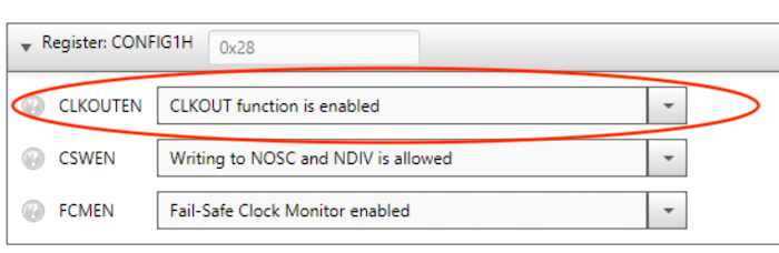
CLKOUTEN - CLKOUT function is enabled
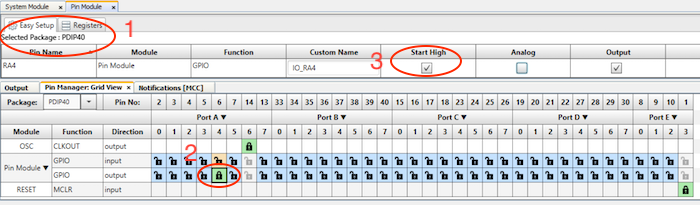
That completes the inputs needed in the System Module. Next click on the Pin Module tab in the editor pane. Note that again there are two sub-tabs: Easy Setup and Registers. Also note that there is a Pin Manager: Grid View tab in the pane below the editor pane (note that these screens show the pane arrangement with a default IDE configuration – if you have opened / closed other windows, you may need to open the necessary windows via the Window menu).
Ensure the correct package is selected in the Pin Manager: Grid View Package: drop down – PDIP40. There are initially no pins available for editing in the Easy Setup sub-tab – a pin needs to be selected in the Pin Manager: Grid View first. As we have enabled the CLKOUT function, the Port A Bit 6 (RA6)- Pin 14 - is now configured as CLKOUT / output in the Pin Manager Grid View and it has a green lock indicating that it is currently in use. Click on the open lock of the Port A Bit 4, GPIO / output in the Pin Manager Grid View which changes the icon in that row to a green locked lock. Also note that Pin RA4 is now available for editing in the Easy Setup sub-tab. Click the Start High checkbox to set the initial value of the GPIO to high thereby lighting up the LED. When done, the Pin Module should appear as:
The required configuration is complete. Click the Generate button in the Resource Management (MCC) tab (in the left pane of the IDE) to have MCC generate and insert the necessary code in the current project.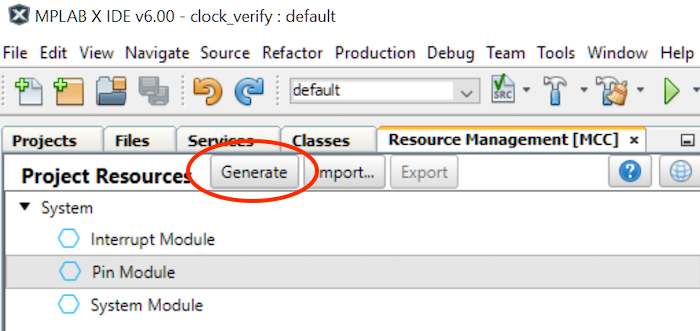
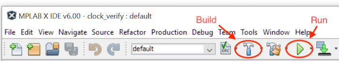
Build and Run
The project can now be built, uploaded to the microcontroller, and run. The Run button on the toolbar both builds and if the build succeeds, programs the PIC®. I prefer to keep the two as separate operations and almost always click Build and then Run(which builds the application again!). The related buttons are highlighted below:
Regardless of how you get there, you should see both a build output:
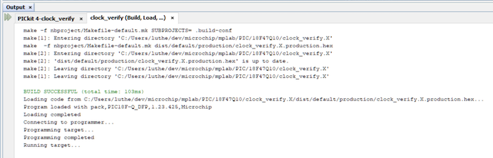
And a load output...
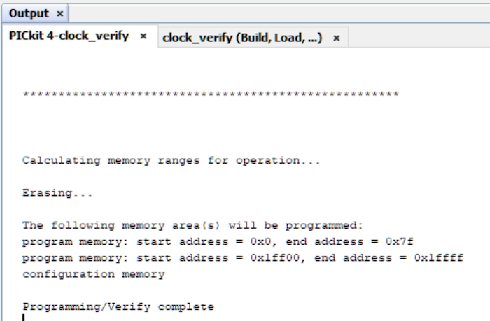
Once upload is complete, the LED lights. The clock output on RA6 can also be verified.
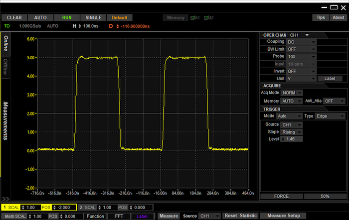
Note that the oscilloscope trace capturing the clock output has a period of 500nS (2MHz) while the configuration set the clock speed to 8 MHz. Looking at the processor data sheet, for the config1 register, when the CLKOUT function is enabled, OSC2 (RA6) outputs the clock / 4.
Summary
This post started with a high-level overview of Microchip’s PIC® line of microprocessors and a quick tour of available options to start 8-bit PIC® development. Efforts then moved to building a simple circuit on a breadboard around a a PDIP version of the PIC18F47Q10 and connected a stand alone MPLAB® PICkit™ 4 programmer/debugger. With the hardware in place, the next task was installing Microchip’s tooling, including MPLAB® X Integrated Development Environment and MPLAB®Code Configurator to configure the PIC18F47Q10’s clock system and GPIO pins. The discussion wrapped up with building the solution, flashing the processor, and validating the configuration through the system clock output and a lighting a discrete LED on the breadboard. With this work completed, we are in position to start diving deeper into various 8-bit PIC® peripherals such as GPIO, timers and interrupts.


- Comments
- Write a Comment Select to add a comment
To post reply to a comment, click on the 'reply' button attached to each comment. To post a new comment (not a reply to a comment) check out the 'Write a Comment' tab at the top of the comments.
Please login (on the right) if you already have an account on this platform.
Otherwise, please use this form to register (free) an join one of the largest online community for Electrical/Embedded/DSP/FPGA/ML engineers:


