


This is a short article explaining how to analyze part of the behavior of a power MOSFET during turn-on, and how it is influenced by the parasitic inductance at the source terminal. Parasitic inductance is not a good thing — the word parasite in biology refers to an external thing that feeds off a host organism; while parasitic elements in electronics are a little different, they are still undesirable by their nature and not part of any intended feature. The brief qualitative reason that source inductance is undesirable is that it uses up voltage when current starts increasing during turn-on (remember, \( V = L \frac{dI}{dt} \)), voltage that would otherwise be available to turn the transistor on faster. But I want to show a quantitative approximation to understand the impact of additional source inductance, and I want to compare it to the effects of extra inductance at the gate or drain.
I’m going to look at the gate drive circuit shown below. A typical half-bridge — pretend that the lower transistor Q1L is off, that we have just turned off the upper transistor Q1H, and that the body diode of the upper transistor Q1H is conducting some load current \( I_L \). Now we are going to turn on the lower transistor Q1L by applying a voltage step \( V_{g0} \) across the gate through some resistance \( R_1. \) What happens?
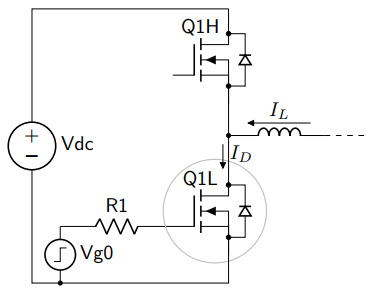
We need a model of the MOSFET. I’ll leave the in-depth discussion for another article, but the basic idea is that the drain current \( I_D \) is dependent on the gate-to-source voltage \( V_{gs} \), which can be modeled as the voltage across a capacitance \( C_{gs} \). To turn it on, you have to start charging up \( C_{gs} \). and once the voltage gets past a threshold voltage of the MOSFET, it starts to conduct, with the drain current increasing until all of the load current \( I_L \) goes through the transistor, and the body diode of Q1H can stop conducting.
That’s the general idea, at least. There are some complicating factors, though, and one of them is the parasitic inductances of the transistor. We can use a more detailed circuit model of the transistor as it connects to the gate (G), source (S), and drain (D) terminals:

Here I haven’t shown the body diode of the lower transistor (for this article we can assume it is not conducting), but the transistor has three parasitic capacitances \( C_{GS}, C_{DS}, C_{DG} \) (often shown as \( C_{GD} \)) inherent in the transistor itself, three parasitic inductances \( L_G, L_S, L_D \) in the packaging leads, and a parasitic gate resistance \( R_G \).
What I will show is that the source inductance \( L_S \) is a critical value that affects turn-on time, with higher inductance slowing down turn-on. Extra circuit trace inductance on a printed circuit board adds to this inductance, so it is generally undesirable, and should be minimized.
I will also give an approximation for determining the first two intervals of turn-on time, with a simplified model:

In the first interval, the voltage across the gate capacitance \( C_{GS} \) increases exponentially toward the gate drive voltage \( V_{g0} \) with time constant
$$\tau \approx (R_1 + R_G)C_{GS} + (L_G + L_S)/(R_1 + R_G),\tag{S1}$$
taking a total time of approximately
$$t_1 = \tau \ln \frac{V_{g0}}{V_{g0}-V_{GS1}} \tag{S2}$$
where \( V_{GS1} \) is the gate voltage required to reach a noticeable drain current \( I_{D0} \) — I’d typically use somewhere between 10 mA and 100 mA, depending on the supply voltage. It’s basically the minimum amount of drain current you might be worried about. Transistor data sheets give a threshold voltage, usually based on 250 μA or 1mA, but that’s too small of a current to care about in most cases.
In the second interval, drain current increases roughly linearly to the load current \( I_L \), with the applied gate drive voltage going to three series elements:
- Gate voltage \( V_{CGS} \) increasing from \( V_{GS1} \to V_{GS2} \) needed to bring the drain current from the small but noticeable \( I_{D0} \) to the load current \( I_L \)
- Inductive drop \( V_L = L_S \dfrac{\Delta I_D}{\Delta t} \)
- Resistive drop \( I_G (R_1 + R_G) \) — we can relate the resistive drop by computing \( I_G = C\frac{dV_C}{dt} \). Here we have two choices:
- We can focus only on gate-to-source capacitance \( C_{GS} \), and neglect gate-to-drain capacitance \( C_{GD} \)
- We can include gate-to-drain capacitance \( C_{GD} \)
The resulting equations are either:
$$\begin{align} I_G (R_1 + R_G) &\approx (R_1 + R_G)C_{GS}(V_{GS2} - V_{GS1})/\Delta t \tag{S3} \\ I_G (R_1 + R_G) &\approx (R_1 + R_G)\left(C_{GS}(V_{GS2} - V_{GS1}) - C_{DG}(V_{CDG2} - V_{CDG1})\right)/\Delta t \tag{S4} \\ \end{align}$$
The change in drain-to-gate voltage is primarily due to drain inductance:
$$\Delta V_{CDG} = V_{CDG2} - V_{CDG1} \approx -L_D\frac{\Delta I_D}{\Delta t} \tag{S5}$$
We can solve for \( \Delta t = t_2 - t_1 \) assuming gate voltage is roughly the average value \( (V_{GS1}+V_{GS2})/2 \).
The voltage equation, when we put everything together (based on equations S4 and S5), is:
$$V_{g0} \approx \underbrace{\frac{V_{GS1}+V_{GS2}}{2}} _ {C_{GS}\ \text{voltage}} + \underbrace{\frac{L_S I_L}{\Delta t}} _ {L_S\ \text{voltage}} + \underbrace{\frac{(R_1 + R_G)\left(C_{GS}(V_{GS2} - V_{GS1}) + \dfrac{C_{DG}L_DI_L}{\Delta t}\right)}{\Delta t}} _ {IR\ \text{voltage}} \tag{S6}$$
The easier case is to neglect gate-to-drain capacitance and drain inductance — set \( C_{DG}{L_D} = 0 \), and solve for \( \Delta t: \)
$$\Delta t = t_2 - t_1 \approx \frac{L_S I_L + (R_1 + R_G)C_{GS}(V_{GS2} - V_{GS1})}{V_{g0} - (V_{GS1}+V_{GS2})/2} \tag{S7}$$
Otherwise we have a quadratic equation in \( \Delta t \), which we can solve with the quadratic formula, using the more positive root:
$$\begin{align} 0 &= A(\Delta t)^2 + B\Delta t + C \\ A &= V_{g0} - (V_{GS1}+V_{GS2})/2 \\ B &= - L_S I_L - (R_1 + R_G)C_{GS}(V_{GS2} - V_{GS1})\\ C &= -(R_1 + R_G)C_{DG}L_DI_L \\ \Delta t &= \frac{-B + \sqrt{B^2 - 4AC}}{2A} \end{align}\tag{S8}$$
Setting \( C=0 \) produces a decreased value of \( \Delta t \) equal to the value in equation S7.
In either case this second time interval \( \Delta t \) is dominated by the effects of \( L_S \) — most of the gate voltage is required across the source inductance in order to increase the transistor drain current, and the IR drop is relatively small.
These simplified equations S1 - S8 are easy to calculate, and you don’t have to mess with more complicated models. Also, unless you’re dealing with a really badly-designed circuit board with high parasitic inductance, the resulting time intervals are short, and turn-on will be dominated by charging the Miller capacitance \( C_{DG} \), which I’ll cover in another article. So the accuracy doesn’t have to be very good anyway; we’re just looking for something that’s within maybe 20% of the real value.
A more complex solution involves the way the voltages and currents change over time — which means we are entering the world of numerical solutions of differential equations.
As an example case, we’ll use the IRL640 — a rather ancient part, but I have my reasons.
Where to start?
We can simulate this circuit by solving differential equations for four state variables in this circuit, namely the currents \( I_G \) and \( I_S \) through the inductances, and the voltages \( V_{CGS} \) and \( V_{CDS} \) across the capacitances. (\( I_D \) and \( V_{GD} \) are dependent voltages: \( I_G + I_D = I_S \) and \( V_{CGS} + V_{CGD} = V_{CDS}. \))
I will try to keep from getting stuck in too much Grungy Algebra, but to some extent it’s unavoidable. Here’s how to get to a set of four state variable equations:
We start with some basic circuit equations from Kirchhoff’s current and voltage laws:
$$\begin{align} I_S &= I_{CGS} + I_T + I_{CDS} \tag{1} \\ I_D &= I_{CDG} + I_T + I_{CDS} \tag{2} \\ V_{CDG} &= V_{CDS} - V_{CGS} \tag{3} \\ \frac{I_{CDG}}{C_{DG}} &= \frac{I_{CDS}}{C_{DS}} - \frac{I_{CGS}}{C_{GS}} \tag{4} \end{align}$$
The first two equations cover the way the current splits into capacitor currents at the drain and source of the MOSFET, once you get past the lead inductances. The last two equations relate to the capacitor voltages: equation 3 shows how the capacitor voltages relate, and if we take the derivative and replace \( dV_{Cx}/dt = I_{Cx}/{C_x} \) for each capacitor \( C_x \), we get Equation 4.
Combine Equations 4 and 2:
$$\begin{align} I_D &= C_{DG}\left(\frac{I_{CDS}}{C_{DS}} - \frac{I_{CGS}}{C_{GS}}\right) + I_T + I_{CDS} \\ &= \frac{C_{DG}}{C_{DS}}I_{CDS} - \frac{C_{DG}}{C_{GS}}I_{CGS} + I_T + I_{CDS} \tag{5} \end{align}$$
Eliminate \( I_{CGS} = I_S - I_T - I_{CDS} \) from Equation 1:
$$I_D = \frac{C_{DG}}{C_{DS}}I_{CDS} - \frac{C_{DG}}{C_{GS}}\left(I_S - I_T - I_{CDS}\right)+ I_T + I_{CDS} \tag{6}$$
Collect terms and solve for \( I_{CDS} \):
$$I_D = \left(\frac{C_{DG}}{C_{DS}} + \frac{C_{DG}}{C_{GS}} + 1\right) I_{CDS} + \left(\frac{C_{DG}}{C_{GS}} + 1\right)I_T - \frac{C_{DG}}{C_{GS}}I_S \tag{7}$$
$$I_{CDS} = C_{DS}\frac{dV_{CDS}}{dt} = \frac{I_D + \frac{C_{DG}}{C_{GS}}I_S - \left(\frac{C_{DG}}{C_{GS}} + 1\right)I_T} {\frac{C_{DG}}{C_{DS}} + \frac{C_{DG}}{C_{GS}} + 1} \tag{8}$$
This we can use to simulate \( dV_{CDS}/dt \); the currents \( I_D \) and \( I_S \) are state variables, and the transistor current \( I_T \) is a function of the state variable \( V_{CGS} \).
Now we can do something similar with Equation 5 to eliminate \( I_{CDS} = I_S - I_T - I_{CGS} \) from Equation 1:
$$I_D = \frac{C_{DG}}{C_{DS}}\left(I_S - I_T - I_{CGS}\right) - \frac{C_{DG}}{C_{GS}}I_{CGS} + I_T + I_S - I_T - I_{CGS} \tag{9}$$
Collect terms and solve for \( I_{CGS} \):
$$I_D = \left(\frac{C_{DG}}{C_{DS}} + 1\right)I_S - \frac{C_{DG}}{C_{DS}}I_T - \left(\frac{C_{DG}}{C_{DS}} + \frac{C_{DG}}{C_{GS}} + 1\right) I_{CGS} \tag{10}$$
$$I_{CGS} = C_{GS}\frac{dV_{CGS}}{dt} = \frac{\left(\frac{C_{DG}}{C_{DS}} + 1\right)I_S - \frac{C_{DG}}{C_{DS}}I_T - I_D} {\frac{C_{DG}}{C_{DS}} + \frac{C_{DG}}{C_{GS}} + 1} \tag{11}$$
This we can use to simulate \( dV_{CGS}/dt \) as a function of state variables.
We can take a similar approach to determine the voltage across the inductances.
$$\begin{align} V_{dc} &= V_{LD} + V_{CDS} + V_{LS} \tag{12} \\ V_{g0} &= V_{LG} + I_G R + V_{CGS} + V_{LS} \tag{13} \\ I_G &= I_S - I_D \tag{14} \\ \frac{V_{LG}}{L_G} &= \frac{V_{LS}}{L_S} - \frac{V_{LD}}{L_D} \tag{15} \end{align}$$
The first two equations cover the voltage drops between drain and source (totalling \( V_{dc} \)) and across the gate drive circuit (totalling \( V_{g0} \)), including the lead inductances and the external resistance \( R_1 \). (I’ve lumped the resistances together as \( R_1 + R_G = R \).) The last two equations relate to the inductor currents: equation 14 shows how the inductor currents relate, and if we take the derivative and replace \( dI_{Lx}/dt = V_{Lx}/{L_x} \) for each inductor \( L_x \), we get equation 15.
Combine Equations 13 and 15:
$$\begin{align} V_{g0} &= L_G\left(\frac{V_{LS}}{L_S} - \frac{V_{LD}}{L_D}\right) + I_G R + V_{CGS} + V_{LS} \\ &= \frac{L_G}{L_S}V_{LS} - \frac{L_G}{L_D}V_{LD} + I_G R + V_{CGS} + V_{LS} \tag{16} \end{align}$$
Eliminate \( V_{LD} = V_{dc} - V_{CDS} - V_{LS} \) from Equation 12:
$$V_{g0} = \frac{L_G}{L_S}V_{LS} - \frac{L_G}{L_D}\left(V_{dc} - V_{CDS} - V_{LS}\right) + I_G R + V_{CGS} + V_{LS} \tag{17}$$
Collect terms, substitute in \( I_G = I_S - I_D \), and solve for \( V_{LS} \) as a function of state variables:
$$V_{g0} = \left(\frac{L_G}{L_S} + \frac{L_G}{L_D} + 1\right)V_{LS} - \frac{L_G}{L_D}\left(V_{dc} - V_{CDS}\right) + I_G R + V_{CGS} \tag{18}$$
$$V_{LS} = L_S\frac{dI_S}{dt} = \frac{V_{g0} + \frac{L_G}{L_D}V_{dc} - \frac{L_G}{L_D}V_{CDS} - (I_S - I_D)R - V_{CGS}} {\frac{L_G}{L_S} + \frac{L_G}{L_D} + 1} \tag{19}$$
Finally, starting from Equation 16, eliminate \( V_{LS} = V_{dc} - V_{CDS} - V_{LD} \) from Equation 12:
$$V_{g0} = \frac{L_G}{L_S}\left(V_{dc} - V_{CDS} - V_{LD}\right) - \frac{L_G}{L_D}V_{LD} + I_G R + V_{CGS} + V_{dc} - V_{CDS} - V_{LD} \tag{20}$$
Collect terms, substitute in \( I_G = I_S - I_D \), and solve for \( V_{LD} \) as a function of state variables:
$$V_{g0} = -\left(\frac{L_G}{L_S} + \frac{L_G}{L_D} + 1 \right)V_{LD} + \left(\frac{L_G}{L_S} + 1\right)\left(V_{dc} - V_{CDS}\right) + (I_S - I_D) R + V_{CGS} \tag{21}$$
$$V_{LD} = L_D\frac{dI_D}{dt} =
\frac{\left(\frac{L_G}{L_S} + 1\right)\left(V_{dc} - V_{CDS}\right) + (I_S - I_D) R + V_{CGS} - V_{g0}}
{\frac{L_G}{L_S} + \frac{L_G}{L_D} + 1}
\tag{22}$$
We can take Equations 8, 11, 19, and 22, and use them with a differential equation solver.
Now all we need is to figure out transistor current \( I_T \) as a function of voltage \( V_{CGS} \), which in many cases we can get from the transistor datasheet. Here’s the appropriate figure from the IRL640 datasheet:
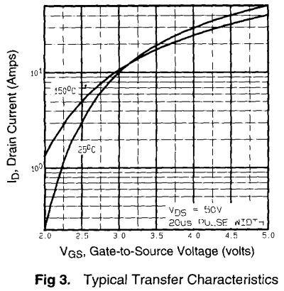
I’m going to digitize the 25°C curve with WebPlotDigitizer, as I did in another recent article.
import numpy as np
import matplotlib.pyplot as plt
%matplotlib inline

# IRL640 fig 3 (25 C curve) digitized

fig3data = np.array([[float(num) for num in line.split(',')]
                 for line in """
2.007416563658838, 0.12161170279284636
2.070457354758962, 0.20961799924531258
2.139060568603214, 0.3462652161722368
2.1946847960444993, 0.5389234652322444
2.2447466007416566, 0.7970358068305596
2.3040791100123608, 1.1296805852833385
2.3597033374536465, 1.5344777344891432
2.419035846724351, 1.9806057227184222
2.4709517923362174, 2.4499801268577173
2.5321384425216316, 3.2028888819877124
2.5896168108776267, 4.08166576143854
2.689740420271941, 5.834583402071244
2.788009888751545, 7.725578939550294
2.8992583436341164, 10.316842440768006
3.1254635352286773, 16.54230634125394
3.327564894932015, 23.346759038331605
3.5444993819530284, 31.44393905230773
3.7614338689740423, 40.242022815960155
4.119283065512979, 56.55396440887105
4.377008652657602, 69.06940492102076
4.695920889987639, 85.80202485397552
4.929542645241038, 97.89568436909394
""".splitlines()
                 if line.strip() != ""])
ii = slice(None,-4)
Vgs = fig3data[ii,0]
Id = fig3data[ii,1]
p = np.polyfit(Vgs,Id,2)
ka,kb,kc=p
x0 = -kb/ka/2
y0 = ka*x0*x0 + kb*x0 + kc
def fquad(x):
return ka*(x-x0)**2 + y0
plt.plot(Vgs,Id,'.',)
plt.plot(Vgs,fquad(Vgs))
plt.plot(Vgs,np.polyval(p,Vgs))
plt.title('%.3f(Vgs-%.3f)^2 + %.3f' % (ka,x0,y0));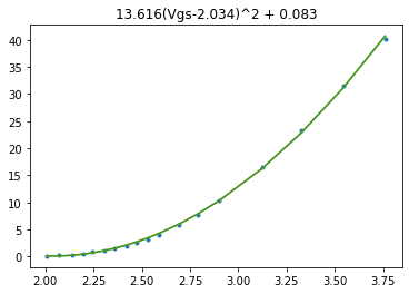
No surprise, we’ve got a quadratic behavior — MOSFETs are supposed to have this quadratic behavior when acting as a current source: \( I_D \propto \left(V_{GS} - V_{TH}\right)^2 \)
The offset term in this best fit (0.083 A) is close enough to zero that I’m just going to ignore it for now, along with any subthreshold behavior; if \( V_{GS} < V_{TH} \) I’m just going to assume there’s zero current.
We also need some system parameters (which I’m just going to pick arbitrarily) and some MOSFET parameters from the datasheet. Here are the system parameters:
- Vdc = 60 V
- Vg0 = 10 V
- Iload = 5 A
- R1 = 14.5 Ω
As for the MOSFET parameters, some are in the datasheet directly, and others we’ll just have to estimate. The capacitances when the drain-to-source voltage is at 60V we can estimate from Figure 5, all the way at the right end of the x-axis:
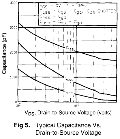
- Cdg ≈ 50 pF
- Cds ≈ 200 pF
- Cgs ≈ 1700 pF
The datasheet gives us typical numbers of 1800 pF, 400 pF, and 120 pF at Vds = 25 V, but the capacitances will be a bit lower at a higher voltage.

The datasheet also gives typical values of inductances for Ld and Ls, which are much more dependent on the packaging rather than the die itself. It doesn’t give a typical value of Lg, but we’ll just use Lg = Ls as an estimate; if you’ve ever opened up a TO-220 package, the gate and source leads are attached to the die with bond wires, whereas the drain is the oddball, with lead connected directly to the die, for a lower inductance.
- Ld ≈ 4.5 nH
- Ls ≈ 7.5 nH
- Lg ≈ 7.5 nH
This data sheet doesn’t give an internal gate resistance, but other MOSFETs typically seem to offer approximately 1 ohm internal gate resistance (NTP185N60S5H = 0.9 Ω, STP30NM30N = 1.7 Ω, PSMN027-100PS = 0.92 Ω), and since I’ve got an external resistance of 14.5 Ω I’m just going to assume the internal gate resistance is zero. Close enough.
Now let’s have the computers do the grungework:
"""
Code in this notebook is copyright 2024 Jason M. Sachs

Licensed under the Apache License, Version 2.0 (the "License");
you may not use this file except in compliance with the License.
You may obtain a copy of the License at

    http://www.apache.org/licenses/LICENSE-2.0

Unless required by applicable law or agreed to in writing, software
distributed under the License is distributed on an "AS IS" BASIS,
WITHOUT WARRANTIES OR CONDITIONS OF ANY KIND, either express or implied.
See the License for the specific language governing permissions and
limitations under the License.
"""

import argparse
import scipy.optimize

def linsolver(f,y0,t,p=None,return_dydt=False):
    """
    Trapezoidal integration over a series of time intervals

    t = time
    y0 = initial value of unknown variable y
    f = function returning dy/dt = f(y,t,p)
    p = parameter object

    Returns a series of values y over the specified time
    return_dydt=True will also return the estimated dy/dt
    """
    yi = y0
    N = len(t)
    y = np.zeros((N,len(y0)))
    dydt = y*0
    tprev = t[0]
    dydt_prev = np.array(f(y[0,:],tprev,p))
    for i in range(N):
        ti = t[i]
        dt = ti-tprev
        # find out dy/dt based on the beginning of the interval
        dydti_1 = dydt_prev
        y_tmp = yi + dydti_1 * dt
        # find out dy/dt based on the end of the interval and the first dy/dt
        dydti_2 = np.array(f(y_tmp,ti,p))
        dydti = (dydti_1 + dydti_2) / 2
        yi += dydti * dt
        y[i,:] = yi
        # save the dydt based on the end of the interval
        # for the beginning of the next interval
        dydt_prev = np.array(f(yi,ti,p))
        dydt[i,:] = dydt_prev
        tprev = ti
    if return_dydt:
        return y, dydt
    else:
        return y

def f_I(Vgs, Vds, p):
    # IRL640 model
    Vth = 2.034
    Vdspos = np.maximum(Vds,0)
    Vq = np.minimum(Vdspos, Vgs-Vth)
    Id_raw = 13.616 * (2*(Vgs-Vth)-Vq)*Vq*(Vgs>Vth)
    return np.minimum(Vdspos/p.Rdson, Id_raw)

def solve_for_I(I, Vds, p, Vgsrange):
    def g(Vgs):
        return f_I(Vgs, Vds, p) - I
    return scipy.optimize.brentq(g, Vgsrange[0], Vgsrange[1])

# State variables = 4x1 array:
# 0. Vcgs
# 1. Vcds
# 2. Is
# 3. Id

def f_IRL640_on(y,t,p):
    Vcgs = y[0]
    Vcds = y[1]
    Is   = y[2]
    Id   = y[3]
    It   = f_I(Vcgs, Vcds, p)

    Cdenom = (p.Cdg/p.Cds + p.Cdg/p.Cgs + 1)
    Icds = (Id + p.Cdg/p.Cgs*Is - (p.Cdg/p.Cgs + 1)*It) / Cdenom
    if Vcds <= It * p.Rdson:
        # A twist: VCds can't be less than It * Rdson
        # If so, It as required to make Vcds =
        Kfudge1 = 1.0 # arbitrary number
        Icds = -Kfudge1*(Vcds - It*p.Rdson)
        It = ((Cdenom*Icds) - Id - (p.Cdg/p.Cgs*Is))/(p.Cdg/p.Cgs + 1)

    Icgs = (-Id - p.Cdg/p.Cds*It + (p.Cdg/p.Cds + 1)*Is) / Cdenom
    Ldenom = (p.Lg/p.Ls + p.Lg/p.Ld + 1)
    # One more twist:
    # Drain current can't be more than the load current.
    # Case 1: drain current < load current: Vds = Vdc

    Vdrop1 = (Is-Id)*p.Rg + Vcgs - p.Vg0
    VLd1 = ((p.Lg/p.Ls+1)*(p.Vdc - Vcds) + Vdrop1) / Ldenom
    # Case 2: drain current >= load current: VLd as required to make Id = Iload
    Kfudge2 = 1  # arbitrary number
    VLd2 = -Kfudge2*(Id - p.Iload)

    if Id <= p.Iload:
        Vdc_minus_Vcds = (p.Vdc - Vcds)
        VLd = VLd1
    else:
        Vdc_minus_Vcds = (VLd2 * Ldenom - Vdrop1)/(p.Lg/p.Ls+1)
        VLd = VLd2
    VLs = (p.Vg0 + p.Lg/p.Ld*Vdc_minus_Vcds - (Is-Id)*p.Rg - Vcgs) / Ldenom
    # Don't allow the drain current to exceed the load current
    return [Icgs/p.Cgs, Icds/p.Cds, VLs/p.Ls, VLd/p.Ld]

def plot_data(t,ydict,params):
    axheights = [0.5,1,1]
    fig,axes = plt.subplots(nrows=3,figsize=(8,7),
                           gridspec_kw=dict(height_ratios=axheights,
                                            hspace=0.07))

    labels = ['VCgs','VCds','Id','It','Ig','Is']
    #imax = int(np.nonzero(y[:,3]>Iload)[0][0] *1.8)
    Vcds_stop = 5.0
    imax = int(np.nonzero(y[:,1]<Vcds_stop)[0][0])
    # stop at Vcds = Vcds_stop arbitrarily
    tscale = t[:imax]*1e9
    for k in range(len(labels)):
        label=labels[k]
        yk = ydict[label][:imax]
        if label.endswith('gs'):
            ax = axes[2]
        elif label.startswith('I'):
            ax = axes[1]
        else:
            ax = axes[0]
        ax.plot(tscale,yk,label=labels[k])
    VCgs = ydict['VCgs'][:imax]
    VCds = ydict['VCds'][:imax]
    VLs = ydict['VLs'][:imax]
    VRg = ydict['Ig'][:imax]*params.Rg
    VLd = ydict['VLd'][:imax]
    VLg = ydict['VLg'][:imax]
    Vg1 = VCgs + VLs
    Vg2 = VCgs + VLs + VLg
    Vg3 = VCgs + VLs + VLg + VRg
    axes[2].fill_between(tscale,VCgs,Vg1, color='#fff8c0',label='VLs')
    axes[2].fill_between(tscale,Vg1,Vg2,
                         color='#d8f8b0',label='VLg')
    axes[2].fill_between(tscale,Vg2,Vg3,
                         color='#d0e0ff',label='IgRg')
    for V in [Vg1, Vg2]:
        axes[2].plot(tscale, V, '--', color='black',
                     linewidth=0.5, dashes=[15,5])
    Vg0_expected = VCgs + VLs + VLg + VRg
    Vdc_expected = VLd + VCds + VLs
    Vg0_dev = np.abs(Vg0_expected - params.Vg0)
    Vdc_dev = np.abs(Vdc_expected - params.Vdc)
    assert(Vg0_dev.max() < 1e-12)
    #assert(Vdc_dev.max() < 1e-12)

    # Highlight turnon steps
    # 1. When It is first > 0.05 A
    # 2. When Id is within 0.05A of load current
    i1 = np.nonzero(ydict['It'] > 0.05)[0][0]
    i2 = np.nonzero(ydict['Id'] > params.Iload - 0.05)[0][0]
    t1 = tscale[i1]
    t2 = tscale[i2]

    # Simplified turn-on model: tau = RgCgs + (Lg+Ls)/Rg
    tau = params.Cgs * params.Rg + (params.Lg+params.Ls) / params.Rg
    # Vcgs for 0.05A and load current
    Vcgs1 = solve_for_I(0.05, params.Vdc, params, [0, 10])
    Vcgs2 = solve_for_I(params.Iload, params.Vdc, params, [0, 10])
    # 1. exponential rise
    t1est = tau*np.log(params.Vg0/(params.Vg0-Vcgs1))
    # 2. Id rises linearly, with VL = Vg0 - Vcgs_avg - Ig * R
    #    Ig = Cgs*delta_v/delta_t
    qA = params.Vg0 - (Vcgs1+Vcgs2)/2
    qB = - params.Ls * params.Iload - params.Rg * params.Cgs * (Vcgs2-Vcgs1)

    delta_t1 = -qB/qA
    # Next more complicated expression for delta_t is to take Cdg and Ld into account,
    # causing a longer time delay:
    qC = - params.Rg * params.Cdg * params.Ld * params.Iload
    delta_t2 = -(qB - np.sqrt(qB*qB - 4*qA*qC))/2/qA

    tapprox0 = np.arange(0,1,0.001)*t1est
    Vgs_est0 = params.Vg0*(1-np.exp(-tapprox0/tau))
    axes[2].plot(tapprox0*1e9, Vgs_est0, color='red',
                     linewidth=1, dashes=[7,2])

    mygreen = '#008000'
    for delta_t, color, label in [
        (delta_t2, mygreen, r'$V_{CGS,\ \text{ideal}}\ (L_D > 0)$'),
        (delta_t1, 'red', r'$V_{CGS,\ \text{ideal}}\ (L_D \approx 0)$')
    ]:
        tapprox1 = np.array([0,delta_t]) + t1est
        Vgs_est1 = Vcgs1 + (Vcgs2-Vcgs1)*(tapprox1-t1est)/delta_t

        axes[2].plot(tapprox1*1e9, Vgs_est1, color=color,
                     marker='.', linewidth=1, dashes=[7,2],
                     label=label)

    tlim = (min(tscale), max(tscale)+tscale[1]-tscale[0])
    if tlim[1] > 100:
        dtick = 10
    if tlim[1] > 50:
        dtick = 5
    elif tlim[1] > 20:
        dtick = 2
    else:
        dtick = 1
    ttick = np.arange(tlim[0],tlim[1]+0.001,dtick)
    for i,ax in enumerate(axes):
        ax.locator_params(nbins=int(10*axheights[i]))
        ax.set_xlim(tlim)
        ax.set_xticks(ttick)
        if ax == axes[-1]:
            pass
        else:
            ax.set_xticklabels([])
        if ax == axes[2]:
            lpos = 'upper left'
        else:
            lpos = None
        ax.legend(labelspacing=0, loc=lpos)
        ax.grid()
        ylim = ax.get_ylim()
        for tk in [t1,t2]:
            ax.plot([tk,tk],ylim,color='black')
        ax.set_ylim(ylim)
    axes[-1].set_xlabel('Time (ns)')
    axes[-1].set_ylabel('Vg')
    return fig,axes
params = argparse.Namespace(
            Cdg = 50e-12,
            Cds = 200e-12,
            Cgs = 1700e-12,
            Ld = 4.5e-9,
            Ls = 7.5e-9,
            Lg = 7.5e-9,
            Rg = 14.5,
            Vg0 = 10,
            Vdc = 60, # complementary diode still carrying current
            Rdson = 0.18,
            Iload = 5
)

def run_solver(t, params):
    y, dydt = linsolver(f_IRL640_on,[0,Vdc,0,0],t,params,return_dydt=True)
    ydict = dict(VCgs=y[:,0], VCds=y[:,1],
                 Is=y[:,2], Id=y[:,3], Ig=y[:,2]-y[:,3],
                 It=f_I(y[:,0],y[:,1],params),
                 VLs=params.Ls*dydt[:,2],
                 VLd=params.Ld*dydt[:,3],
                 VLg=params.Lg*(dydt[:,2]-dydt[:,3]))
    return y,dydt,ydict

t = np.arange(0,100e-9,0.05e-9)
y,dydt,ydict = run_solver(t,params)
fig,axes = plot_data(t,ydict, params)

def params_subtitle(params):
    d = dict(vars(params))
    for k in ['Ls','Lg','Ld']:
        d[k] *= 1e9
    return ('Vdc=%(Vdc).0f V, Vg0=%(Vg0).0f V, '
           +'Rg=%(Rg).1f \u2126, '
           +'Ls=%(Ls).1f nH, Lg=%(Lg).1f nH, Ld=%(Ld).1f nH'
           ) % d
axes[0].set_title('IRL640 turnon simulation, baseline:\n'
                  + params_subtitle(params));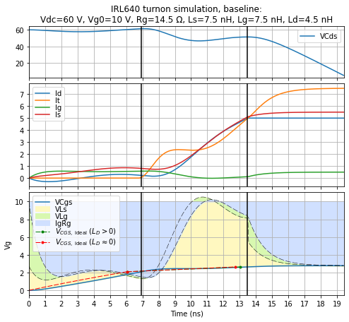
Here I’ve plotted a few things:
- Top subplot: Drain-to-source voltage across the transistor, excluding drain and source inductance
- Middle subplot: Drain, gate, and source currents through the terminals, along with transistor drain current \( I_T \)
- Bottom subplot: Gate capacitance voltage \( V_{CGS} \), along with voltage drops across the source inductance \( L_S \) (yellow), gate inductance \( L_G \) (green), and gate resistance (blue)
- Time intervals:
- First time interval until transistor current starts to rise above zero
- Second time interval until drain current reaches load current
- Third time interval (beyond end of graph) as drain-to-source voltage decreases, charging up the Miller capacitance \( C_{DG} \) — this is beyond the scope of this article, but I’m including it in the graph anyway
- Idealized gate capacitance voltage \( V_{Cgs,\rm{ideal}} \), in dotted red line and dotted green lines, along with calculated intervals based on the equations S1 - S8 that I gave at the beginning of the article for \( t_1 \) and \( t_2 \). The red curve and marker neglects drain inductance; the green curve and marker includes drain inductance.
Here you can see that the approximation for \( t_1 \) and \( t_2 \) isn’t bad, less than 10% off for the total time.
What happens if we try increased values of inductances at each of the terminals?
for whichparam in ['Ls','Ld','Lg']:
    params2 = argparse.Namespace(**vars(params))
    setattr(params2, whichparam, 35e-9)
    t = np.arange(0,100e-9,0.05e-9)
    y,dydt,ydict = run_solver(t,params2)

    fig,axes = plot_data(t,ydict,params2)
    axes[0].set_title('IRL640 turnon simulation, increased %s:\n' % whichparam
                      + params_subtitle(params2));


Here you can see the simplified approximation stays fairly close in two of the three cases — the exception being the case of increased drain inductance, where we need to take \( L_D \) into account with the more quadratic equation to at least stay close to the actual turn-on time.
In the case of increased source inductance, the second turn-on interval is slowed down significantly, with most of the gate voltage going towards \( L_S dI_S/dt \).
In the case of increased drain inductance, the drain voltage across the transistor drops, coupling into the gate voltage, and slowing down things a little bit compared to the base case.
In the case of increased gate inductance, there’s not much change in the turn-on times; the transients are a little less stable as the gate current increases or decreases, but the timing isn’t affected very much.
I’ll run the same kind of simulation for a 15A load:
for whichparam in ['','Ls','Ld','Lg']:
    params2 = argparse.Namespace(**vars(params))
    params2.Iload = 15
    extratitle = ''
    if whichparam != '':
        setattr(params2, whichparam, 35e-9)
        extratitle = ', increased %s' % whichparam
    t = np.arange(0,100e-9,0.05e-9)
    y,dydt,ydict = run_solver(t,params2)

    fig,axes = plot_data(t,ydict,params2)
    axes[0].set_title('IRL640 turnon simulation, Iload = %dA%s:\n' % (params2.Iload, extratitle)
                      + params_subtitle(params2));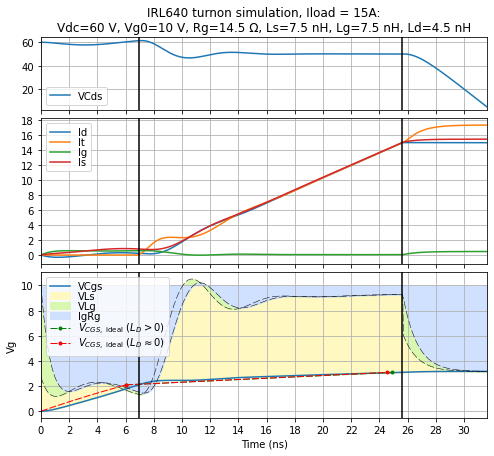
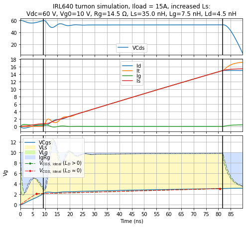
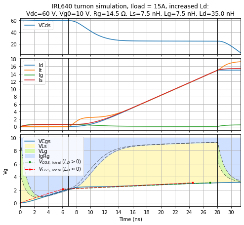

Same general behavior:
- increased gate inductance barely affects the turn-on time
- increased source inductance increases the turn-on time significantly, but its effects are captured well by the simplified model
- increased drain inductance increases the turn-on time slightly, and we need to take \( L_D \) into account in the simplified model, if we want a reasonably accurate approximation.
Nanohenries
The extra inductance I added in these simulations was only about 30 nH, which is relatively small; according to an Analog Devices application note, a 2.54cm trace (1 inch) can add 29nH. The source inductance in a MOSFET gate drive circuit is absolutely critical, and you’ll want to take extra precautions to keep it as small as possible. Spend your time focusing on the source inductance; gate and drain inductance are a little less critical.
Longer turn-on time with current flowing through the MOSFET means more switching losses… you might want to make the turn-on time intentionally a little longer for other reasons, but this should depend on a controlled circuit component that you can adjust as needed, and not parasitic trace inductance.
You’ll also notice in the graphs above that extra source inductance causes more high-frequency ringing in the response. This is undesirable. Keep that source inductance low!
Wrapup
Today we looked at the first two intervals in turn-on time of a MOSFET in a half-bridge with inductive load.
I showed an electrical circuit model, with:
- parasitic capacitances \( C_{GS}, C_{DG}, C_{DS} \)
- parasitic inductances \( L_G, L_D, L_S \)
- internal gate resistance \( R_G \)
I showed a set of equations S1 - S8 for estimating turn-on interval times:
- \( t_1 \) = time for gate capacitance \( C_{GS} \) to charge up enough for current to start to flow and reach some nominal drain current \( I_{D0} \) (see equations S1 and S2)
- \( \Delta t = t_2 - t_1 \) = time for current through the source inductance to increase from \( I_{D0} \) to \( I_L \)
- The simpler equation for \( \Delta t \) (S7) neglects \( C_{GD} \) and \( L_D \), and is an adequate approximation if the drain inductance is small.
- Equation S8 is a quadratic equation that takes \( C_{GD} \) and \( L_D \) into account, replacing equation S7, and is more accurate if the drain inductance is large.
We also looked at a simulation of the turn-on transient, with increased source, gate, and drain inductances. The effect of increased source inductance was the worst, and this should be handled very carefully during board layout.
Further reading
Here are some references covering similar material:
- Vishay AN850: Power MOSFET Basics: Understanding the Turn-On Process
- Infineon AN2203: Gate drive for power MOSFETs in switching applications, Peter B. Green and Liz Zheng, 2022.
- ON Semi TND6237: SiC MOSFETs: Gate Drive Optimization
- ON Semi AND9410: Methods to Characterize Parasitic Inductance and Resistance of Modern VRM, April 2016.
- ON Semiconductor: An Inductive-Switching Loss Model Accounting for Source Inductance and Switching Loop Inductance, Zhiyang Chen, 2014.
- TI seminar 1400 Appendix A: Estimating MOSFET Parameters from the Data Sheet
- Effect of Source Inductance on MOSFET Rise and Fall Times, Alan Elbanhawy, March 2008.
- A Power MOSFET SPICE Model with Built-In Model Generator, Andre Adrian, High Frequency Electronics Magazine, August 2013
- TI Application Report SLPA009A: Power Loss Calculation With Common Source Inductance Consideration for Synchronous Buck Converters, David Jauregui, Bo Wang, and Rengang Chen, July 2011.
- UC Berkeley, EE 105 Spring 2008, Discussion #9: MOSFETs, Ming Wu, 2008.
- Common Source Inductance Introduced Self-turn-on in MOSFET Turn-off Transient, Wen Zhang, Zheyu Zhang, Fred Wang, Daniel Costinett, Leon Tolbert, Benjamin Blalock, APEC 2017.
- Analog Devices: A Practical Guide to High-Speed Printed-Circuit-Board Layout, John Ardizzoni, September 2005.
- Switching Loss Analysis Considering Parasitic Loop Inductance with Current Source Drivers for Buck Converters, Zhiliang Zhang, Jizhen Fu, and Yan-Fei Liu, 2010.
- A Survey on Switching Oscillations in Power Converters, Tianjiao Liu, Thomas T. Y. Wong, and Z. John Shen, 2019.
- Gate Drive Design for SiC MOSFET Device Characterization, Elochukwu Mbah, 2023.
Thanks for reading!
© 2024 Jason M. Sachs, all rights reserved.


