


How to Analyze a Differential Amplifier
There are a handful of things that you just have to know if you do any decent amount of electronic circuit design work. One of them is a voltage divider. Another is the behavior of an RC filter. I'm not going to explain these two things or even link to a good reference on them — either you already know how they work, or you're smart enough to look it up yourself.
The handful of things also includes some others that are a little more interesting to discuss. One of them is this circuit, the differential amplifier.
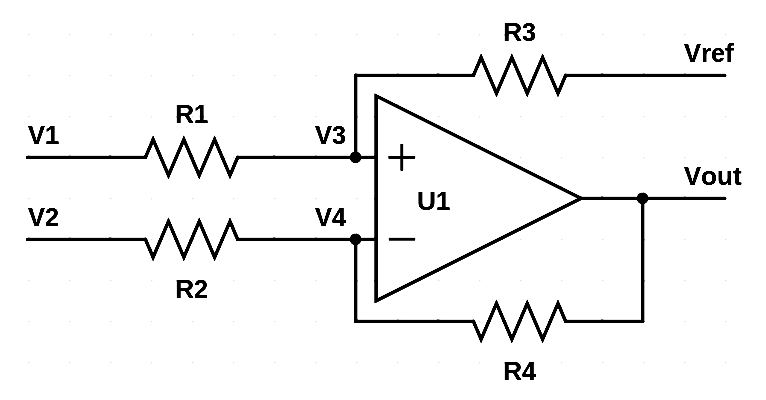
First let's cut to the chase. In case you haven't seen it before, it's a way of amplifying signals. You pick \( R_2 = R_1 = R \) and \( R_4 = R_3 = KR \), and go find a friendly perfect ideal op-amp, and bingo, \( V_\text{out} - V_\text{ref} = K\left(V_1 - V_2\right) \). In other words the voltage between Vout and Vref is K times as much as the voltage between V1 and V2. If you're stuck with some unfriendly voltages V1 and V2, you just stick a differential amplifier there and shazaam, you can see their voltage difference on your terms.
I'm going to say this again, with an example:
Let's say \( V_2 = 40\text{V} + 10\text{V} \sin 377t + f(t) \). That's 40V DC plus 10V at 60Hz AC, plus some other nasty signal f(t) we don't even know about. Heck, maybe f(t) is some Rick Astley song being played in a loop over and over again, loudly. (Never gonna give, never gonna give...) And it's coming from some evil voltage source out of your control. Yuck. And attached to this is a millivolt signal Vsrc that's a secret coded message telling you the location of Jimmy Hoffa's body, Amelia Earhart's airplane, and those 13 paintings stolen in 1990 from the Isabella Stewart Gardner Museum. So \( V_1 = V_2 + V_{src} \), and you have access to V1 and V2. All you have to do is separate the signal from the crap. (Inside we both know what's been going on...) And fame and fortune are yours! A differential amplifier will let you amplify this signal and translate it up or down in voltage relative to any reference you care about, whether it's earth ground or a 2V reference or some other waveform you prefer.
Okay, well, that's the idea, at least. Now it's time for a reality check.
Grungy Algebra
Yes, it's time for everyone's favorite game show, Grungy Algebra!

Today we're going to derive the differential amplifier output voltage formula, with no assumptions on resistor values. Ready? (If this stuff makes you queasy, just skip to the next section. Actually, maybe you should anyway. Come back when you're in a game show mood.)
Okay, first we figure out what the voltage is on node V3. This isn't so bad:
\( V_3 = V_\text{ref} + \frac{R_3}{R_1+R_3} \left(V_1 - V_\text{ref}\right) \)
\( V_3 = \frac{R_1}{R_1+R_3} V_\text{ref} + \frac{R_3}{R_1+R_3}V_1 \)
And the negative terminal path forms an inverting amplifier:
\( V_\text{out} - V_4 = \frac{R_4}{R_2}\left(V_4 - V_2\right) \)
Now, with an ideal op-amp, we know V4 = V3, because we've correctly hooked it up with negative feedback. So now we just have to substitute V4 = V3:
\( V_\text{out} - \frac{R_1}{R_1+R_3} V_\text{ref} - \frac{R_3}{R_1+R_3}V_1 = \frac{R_4}{R_2}\left(\frac{R_1}{R_1+R_3} V_\text{ref} + \frac{R_3}{R_1+R_3}V_1 - V_2\right) \)
And finally, then we simplify:
\( V_\text{out} = V_\text{ref} \left(\frac{R_1}{R_1+R_3} + \frac{R_4}{R_2}\frac{R_1}{R_1+R_3}\right) + \frac{R_4}{R_2}\left( \frac{R_3}{R_1+R_3} V_1 - V_2\right) + \frac{R_3}{R_1+R_3} V_1 \)
\( V_\text{out} = V_\text{ref} \frac{R_1}{R_1+R_3} \left(1 + \frac{R_4}{R_2}\right) + \left(\frac{R_4}{R_2} \frac{R_3}{R_1+R_3} + \frac{R_3}{R_1+R_3} \right) V_1 - \frac{R_4}{R_2}V_2 \)
\( V_\text{out} = V_\text{ref} \frac{1 + R_4/R_2}{1+R_3/R_1} + \left(\frac{R_4}{R_2} +1 \right)\frac{R_3/R_1}{1+R_3/R_1} V_1 - \frac{R_4}{R_2}V_2 \)
\( V_\text{out} = \frac{1 + R_4/R_2}{1+R_3/R_1} \left(V_\text{ref} + \frac{R_3}{R_1}V_1\right) - \frac{R_4}{R_2}V_2 \)
There! Now isn't that enlightening? No?
Well, to make any sense out of this, we have to make a leap of intuition. Here we are dealing with four numbers, \( R_1, R_2, R_3, R_4 \) and they're a muddle. The key here is that we wanted both \( \frac{R_4}{R_2} = K \) and \( \frac{R_3}{R_1} = K \). But that's for perfect resistors, and we can't have perfect resistors. They'll always be a little different from what we wanted. What we'll do is figure out an average gain \( K = \frac{1}{2}\left(\frac{R_3}{R_1} + \frac{R_4}{R_2} \right) \). And the difference will be \( \delta = \frac{1}{2K}\left(\frac{R_3}{R_1} - \frac{R_4}{R_2}\right) \). If you do a little manipulation, then \( \frac{R_3}{R_1} = K\left(1+\delta\right) \) and \( \frac{R_4}{R_2} = K\left(1-\delta\right) \).
Now take a deep breath and plug into our voltage equation:
\( V_\text{out} = \frac{1 + K\left(1-\delta\right)}{1+K\left(1+\delta\right)} \left(V_\text{ref} + K\left(1+\delta\right)V_1\right) - K\left(1-\delta\right)V_2 \)
Hmm, that's not looking much better, is it? Well, what we're trying to do is show that the output voltage is what we expect, plus some error. So let's try to isolate on the good stuff:
\( V_\text{out} = V_\text{ref} + K\left(V_1 - V_2\right) + V_\text{err} \)
\( V_\text{err} = \left( \frac{1 + K\left(1-\delta\right)}{1+K\left(1+\delta\right)} - 1 \right) V_\text{ref} + \left( \frac{1 + K\left(1-\delta\right)}{1+K\left(1+\delta\right)}K\left(1+\delta) - K \right)\right) V_1 - K\left(1-\delta\right)V_2 + KV_2 \)
And now things will start disappearing:
\( V_\text{err} = \left(\frac{1 + K\left(1-\delta\right)}{1+K\left(1+\delta\right)} -1\right)V_\text{ref} + \left(K\left(1+\delta\right)\frac{1+K\left(1-\delta\right)}{1+K\left(1+\delta\right)} -K\right)V_1 + K\delta V_2 \)
\( V_\text{err} = \left(\frac{1 + K\left(1-\delta\right)}{1+K\left(1+\delta\right)} -1\right)V_\text{ref} + \left(K\left(1+\delta\right)\frac{1+K\left(1-\delta\right)}{1+K\left(1+\delta\right)} -K - K\delta\right)V_1 + K\delta V_1 + K\delta V_2 \)
\( V_\text{err} = \left(\frac{1 + K\left(1-\delta\right)}{1+K\left(1+\delta\right)} -1\right)V_\text{ref} + K\left(1+\delta\right) \left(\frac{1+K\left(1-\delta\right)}{1+K\left(1+\delta\right)} - 1\right)V_1 + K\delta V_1 + K\delta V_2 \)
That same term \( \left(\frac{1 + K\left(1-\delta\right)}{1+K\left(1+\delta\right)} -1\right) \) shows up twice. If we simplify it, we get \( \frac{1 + K - K\delta - 1 - K - K\delta}{1+K+K\delta} = \frac{- 2K\delta}{1+K+K\delta} \), so:
\( V_\text{err} = \frac{- 2K\delta}{1+K+K\delta}V_\text{ref} + K\left(1+\delta\right) \frac{- 2K\delta}{1+K+K\delta}V_1 + K\delta V_1 + K\delta V_2 \)
\( V_\text{err} = \frac{- 2K\delta}{1+K+K\delta}V_\text{ref} -2K\delta \frac{K\left(1+\delta\right)}{1+K+K\delta}V_1 + K\delta V_1 + K\delta V_2 \)
\( V_\text{err} = \frac{- 2K\delta}{1+K+K\delta}V_\text{ref} + K\delta \left(1 - \frac{2K\left(1+\delta\right)}{1+K+K\delta}\right)V_1 + K\delta V_2 \)
\( V_\text{err} = \frac{- 2K\delta}{1+K+K\delta}V_\text{ref} + K\delta \frac{1+K+K\delta-2K-2K\delta}{1+K+K\delta}V_1 + K\delta V_2 \)
\( V_\text{err} = \frac{- 2K\delta}{1+K+K\delta}V_\text{ref} + K\delta \frac{1-K-K\delta}{1+K+K\delta}V_1 + K\delta V_2 \)
\( V_\text{err} = \frac{- 2K\delta}{1+K+K\delta}V_\text{ref} + K\delta \left( \frac{1-K-K\delta}{1+K+K\delta}V_1 + V_2\right) \)
And that's about as simple as we can get in terms of Vref, V1, and V2.
Audit time!

Now the problem with everyone's favorite game show, Grungy Algebra!, is that we can make mistakes. In fact I made three or four sign errors before getting it right. So we have to audit our results and make sure they're correct. Let's do it with an example situation.
Let's use \( R_1 = 1\text{K}\Omega, R_2 = 1\text{K}\Omega, R_3 = 10.1\text{K}\Omega, R_4 = 9.9\text{K}\Omega \). We're aiming for a gain of 10, but R3 is 1% high and R4 is 1% low. This gives us K = 10 and \( \delta \) = 0.01.
Let's start back at an early equation and start plugging in numbers:
\( V_\text{out} - \frac{R_1}{R_1+R_3} V_\text{ref} - \frac{R_3}{R_1+R_3}V_1 = \frac{R_4}{R_2}\left(\frac{R_1}{R_1+R_3} V_\text{ref} + \frac{R_3}{R_1+R_3}V_1 - V_2\right) \)
\( V_\text{out} = \frac{R_1}{R_1+R_3} V_\text{ref} + \frac{R_3}{R_1+R_3}V_1 + \frac{R_4}{R_2}\left(\frac{R_1}{R_1+R_3} V_\text{ref} + \frac{R_3}{R_1+R_3}V_1 - V_2\right) \)
\( V_\text{out} = \frac{1}{11.1} V_\text{ref} + \frac{10.1}{11.1}V_1 + 9.9\left(\frac{1}{11.1} V_\text{ref} + \frac{10.1}{11.1}V_1 - V_2\right) \)
\( V_\text{out} = \frac{10.9}{11.1} V_\text{ref} + 10.9 \frac{10.1}{11.1}V_1 - 9.9V_2 \)
\( V_\text{out} \approx 0.981982 V_\text{ref} + 9.918018V_1 - 9.9V_2 \)
\( V_\text{out} = V_\text{ref} + 10\left(V_1-V_2\right) + V_\text{err}\qquad V_\text{err} \approx -0.018018 V_\text{ref} - 0.081982 V_1 + 0.1V_2 \)
Now let's use our error formula:
\( V_\text{err} = \frac{- 2K\delta}{1+K+K\delta}V_\text{ref} + K\delta \left( \frac{1-K-K\delta}{1+K+K\delta} V_1 + V_2\right) \)
\( V_\text{err} = \frac{- 0.2}{1+10+0.1}V_\text{ref} + 0.1 \left(\frac{1-10-0.1}{1+10+0.1} V_1 + V_2\right) \)
\( V_\text{err} = \frac{-0.2}{11.1}V_\text{ref} + 0.1 \left(\frac{-9.1}{11.1}V_1 + V_2\right) \)
\( V_\text{err} \approx -0.018018V_\text{ref} -0.081982V_1 + 0.1V_2 \)
Hurray! Agreement! So there's a pretty good chance we won this round of Grungy Algebra!
So What? (Modal Jazz)
So what? Well, start that Miles Davis album playing and we'll talk about it.
If you look at the error gains (\( -0.018018V_\text{ref} -0.081982V_1 + 0.1V_2 \)) relative to the nominal gains (1, 10, -10), you'll see that they're on the order of \( 2\delta \) for \( V_\text{ref} \), and \( \delta \) for V1 and V2. That's not too bad: if you use 1% resistors, the error is about 1% as well. It's actually better than that, and to see why, we have to talk about normal modes.
I remember my introductory electronics course in college: one of the instructors kept using these words "common-mode" and "differential-mode", and even though he explained how they were defined, it sounded to me like a gimmick. In the differential amplifier, you have inputs V1 and V2, and they're real voltages that are directly measurable.
We can define the common-mode voltage \( V_\text{cm} = \frac{V_1 + V_2}{2} \) and the differential-mode voltage \( V_\text{dm} = V_1 - V_2 \) (or equivalently, \( V_1 = V_\text{cm} + \frac{1}{2}V_\text{dm} \) and \( V_2 = V_\text{cm} - \frac{1}{2}V_\text{dm} \)); neither of these voltages are directly measurable, but they have certain uses in circuit analysis. The point is that real systems have natural or "normal" modes which interact in different ways, and the measurements you can make (voltages V1 and V2 in this case) are usually linear combinations of the normal modes; the normal modes themselves are not directly measurable, but can be calculated as linear combinations of direct measurements. The classical example of this is a coupled pendulum:
Here are two identical pendulums (alternatively, pendula, la-di-da) with the same resonant frequency (defined by gravity and the length of the pendulum) and a weak coupling between them caused by the fact that the strings on which the pendulums are mounted can move and transmit forces to each other. The normal modes in this case are also common-mode and differential-mode. The common-mode is the pendulums moving in sync in the same direction; the differential-mode is the pendulums moving in sync in opposite directions; the two have slightly different resonant frequencies because the connecting string affects the differential mode but not the common mode. Physics students have the task of analyzing this system and writing the equations of motion in terms of the two modes.
Those of you who are into the Zen of Matrices will recognize normal modes as eigenvector/eigenvalue decomposition. If that sparks an idea in your brain, stop and think about it for a while.
Sometimes we use modal analysis not just for the natural dynamics of a system, but for artificial purposes. Common-mode and differential-mode voltages can fall into that category. In a differential amplifier with an ideal op-amp and no filter, there's no dynamic equations that have frequency-dependent terms, so there's no "natural" separation into common-mode and differential-mode dynamics. But we find that common-mode and differential-mode are useful perspectives: common-mode represents the average of two similar circuit voltages or currents. Differential-mode represents the difference of those voltages or currents. In our case, the common-mode voltage has Rick Astley singing loudly (I just wanna tell you how I'm feeling...), whereas the differential-mode voltage has no Rick Astley and contains only the small coded message that's going to tell you where Jimmy Hoffa and Amelia Earhart and the 13 stolen paintings are. We want to get rid of the common-mode voltage. We want to keep the differential-mode voltage.
In three-node systems, we can do something similar called symmetrical components where there are three normal modes: one common-mode signal (called "zero-sequence") and two differential-mode signals that capture the two remaining degrees of freedom — in three-phase systems they are called positive-sequence and negative-sequence.
But we're concerned with a differential-amplifier, a two-node system. Remember: Get rid of Rick Astley (common-mode). Amplify the coded message (differential-mode).
So let's look at the error signal again.
\( V_\text{err} = -0.018018V_\text{ref} -0.081982V_1 + 0.1V_2 \)
We might gain some insight if we write these in terms of common-mode and differential-mode voltages instead of V1 and V2.
\( V_\text{err} = -0.018018V_\text{ref} -0.081982\left(V_\text{cm} + \frac{1}{2}V_\text{dm}\right) + 0.1\left(V_\text{cm} - \frac{1}{2}V_\text{dm}\right) \)
\( V_\text{err} = -0.018018V_\text{ref} + \left(-0.081982 + 0.1\right)V_\text{cm} + \frac{1}{2}\left(-0.081982 - 0.1\right)V_\text{dm} \)
\( V_\text{err} = -0.018018V_\text{ref} + 0.018018V_\text{cm} - 0.090991V_\text{dm} \)
So that's interesting. The error term has the same small coefficient for Vref and Vcm, and a larger coefficient for the differential-mode signal. That's good! Remember, we want the coded message, not Rick Astley. Let's do the analysis in terms of the general expression of error:
\( V_\text{err} = \frac{- 2K\delta}{1+K+K\delta}V_\text{ref} + K\delta \left( \frac{1-K-K\delta}{1+K+K\delta} V_1 + V_2\right) \)
\( V_\text{err} = \frac{- 2K\delta}{1+K+K\delta}V_\text{ref} + K\delta \left( \frac{1-K-K\delta}{1+K+K\delta} \left(V_\text{cm} + \frac{1}{2}V_\text{dm}\right) + \left(V_\text{cm} - \frac{1}{2}V_\text{dm}\right)\right) \)
\( V_\text{err} = \frac{- 2K\delta}{1+K+K\delta}V_\text{ref} + K\delta \left( \left(\frac{1-K-K\delta}{1+K+K\delta} +1 \right)V_\text{cm} + \frac{1}{2}\left(\frac{1-K-K\delta}{1+K+K\delta} - 1\right)V_\text{dm}\right) \)
\( V_\text{err} = \frac{- 2K\delta}{1+K+K\delta}V_\text{ref} + K\delta \left( \frac{2}{1+K+K\delta} V_\text{cm} + \frac{1}{2}\frac{-2K-2K\delta}{1+K+K\delta}V_\text{dm}\right) \)
\( V_\text{err} = \frac{2K\delta}{1+K+K\delta}\left(V_\text{cm} - V_\text{ref}\right) - K\delta \frac{K+K\delta}{1+K+K\delta}V_\text{dm} \)
\( V_\text{err} = \frac{2K\delta}{1+K+K\delta}\left(V_\text{cm} - V_\text{ref} - \frac{K+K\delta}{2}V_\text{dm}\right) \)
Again, same magnitude coefficient for Vref and Vcm. This expression is still a little complex-looking. It may help if we make the approximation that the mismatch \( \delta \) is small, i.e. \( |\delta| \ll 1 \):
\( V_\text{err} \approx \frac{2K\delta}{1+K}\left(V_\text{cm} - V_\text{ref} - \frac{K}{2}V_\text{dm}\right) \)
Now we have something useful and fairly simple. Let's put it in a tabular format.
Output voltage of a differential amplifier
The output voltage of a differential amplifier can be expressed as the sum of linear combinations of Vref, Vcm, and Vdm, with the following coefficients, where the nominal gain \( K = \frac{1}{2}\left(\frac{R_3}{R_1} + \frac{R_4}{R_2} \right) \), and the error factor \( \delta = \frac{1}{2K}\left(\frac{R_3}{R_1} - \frac{R_4}{R_2}\right) \):
| Nominal | Error | |
|---|---|---|
| Vref | 1 | \( \frac{-2K\delta}{1+K+K\delta} \approx -2\delta\frac{K}{1+K} \) |
| Vcm | 0 | \( \frac{2K\delta}{1+K+K\delta} \approx 2\delta\frac{K}{1+K} \) |
| Vdm | K | \( \frac{-K\delta}{1+K+K\delta}\left(K+K\delta\right) \approx -\delta K \frac{K}{1+K} \) |
And here's the thing: we don't really care that much about the error in the reference and differential-mode voltages. These are just small relative gain errors. The only really worrisome term is the common-mode gain, which represents the signal we're trying to keep out (Never gonna say goodbye...) and fortunately does not increase with differential gain K. Whether we have K = 10 or K = 100 or K = 1000, the common mode gain is approximately \( 2\delta \). If we use 1% resistors, the worst-case common-mode gain due to resistor mismatch is 0.04 (when R1 and R4 are too high by 1% and R2 and R3 are too low by 1%).
Non-ideal op-amp characteristics
Well, we talked about using an ideal op-amp in the differential amplifier circuit. Instead we're stuck with a real op-amp.
There are three specs here that affect us the most:
- input and output range
- gain-bandwidth product (GBW)
- input offset voltage and currents
Input and output range is always a concern for any op-amp circuit. Nothing new here. We have to make sure the opamp stays in the linear range, and this requires you to know the specific ranges of input voltages needed for your circuit, along with the specific gains. It's hard to generalize, but not very hard to figure out with specific details. So I won't be covering it.
GBW is easy to figure out: it stays constant, and is the product of circuit gain and circuit bandwidth. If your circuit has a gain of 10, and you're using an op-amp with a GBW of 1MHz, then the overall circuit bandwidth will be 100kHz.
The most interesting aspect here is the effect of offset voltage and currents. The offset voltage Vos causes the diff-amp to act like someone added a small offset to the + input voltage of the opamp. This circuit configuration has a gain from the + node to the output, that is equal to \( \frac{R_4}{R_2}+1 \). This is called the noise gain of the amplifier configuration. Note that it's slightly different than the signal gains.
As for the currents, they come in pairs: there is one current per input (\( I_+ \) and \( I_- \): let's consider positive current being current into the opamp terminals), and therefore they can be expressed as a common-mode and differential-mode current: \( I_\text{cm} = \frac{I_+ + I_-}{2} \) and \( I_\text{dm} = I_+ - I_- \). The common-mode input current is input bias current and the differential-mode input current is input offset current. Input bias current specifications are generally larger than input offset current specifications, at least for bipolar opamps. Modern CMOS opamps have input current specs in the picoamps, and at that level it doesn't usually matter whether the input offset current is smaller.
The positive input current \( I_+ \) has a gain of \( -(R_1 || R_3) = -\frac{R_1R_3}{R_1+R_3} \) to become offset voltage, and then gets multiplied by the noise gain \( \frac{R_4}{R_2} + 1 \). The negative input current \( I_- \) is easier to figure out the gain on the circuit output: it's just R4.
Adding these terms up, we get:
\( \Delta V_\text{out} = (\frac{R_4}{R_2}+1)\left(V_\text{os} - \frac{R_1R_3}{R_1+R_3}I_+\right) + R_4I_- \)
\( \Delta V_\text{out} = \left(1 + K(1-\delta)\right)\left(V_\text{os} - \frac{R_1R_3}{R_1+R_3}I_+\right) + R_4I_- \)
\( \Delta V_\text{out} = \left(1 + K(1-\delta)\right)\left(V_\text{os} - \frac{1}{1+R_3/R_1}R_3I_+\right) + R_4I_- \)
\( \Delta V_\text{out} = \left(1 + K(1-\delta)\right)\left(V_\text{os} - \frac{1}{1+K(1+\delta)}R_3I_+\right) + R_4I_- \)
And here we need one more leap of intuition. The gain mismatch term \( \delta \) only covers the difference between \( \frac{R_3}{R_1} \) and \( \frac{R_4}{R_2} \). We don't have anything that describes the mismatch in impedance in the + terminals and the - terminals; we could multiply R1 and R3 by 10 and it would not affect signal gains, but it will have an effect on the way input currents show up in the output voltage. Let's define \( R_f = \frac{R_3 + R_4}{2} \) and \( \epsilon = \frac{R_3 - R_4}{2R_f} \), so that we can write \( R_3 = R_f \left(1+\epsilon\right) \) and \( R_4 = R_f \left(1-\epsilon\right) \).
\( \Delta V_\text{out} = \left(1 + K(1-\delta)\right)\left(V_\text{os} - \frac{1}{1+K(1+\delta)}R_f\left(1+\epsilon\right)I_+\right) + R_f\left(1-\epsilon\right)I_- \)
\( \Delta V_\text{out} = \left(1 + K(1-\delta)\right)V_\text{os} - \frac{1 + K(1-\delta)}{1+K(1+\delta)}R_f\left(1+\epsilon\right)I_+ + R_f\left(1-\epsilon\right)I_- \)
\( \Delta V_\text{out} = \left(1 + K(1-\delta)\right)V_\text{os} - \frac{1 + K(1-\delta)}{1+K(1+\delta)}R_f\left(1+\epsilon\right)\left(I_\text{cm} + \frac{1}{2}I_\text{dm}\right) + R_f\left(1-\epsilon\right)\left(I_\text{cm} - \frac{1}{2}I_\text{dm}\right) \)
Oh, horrors! We're in Grungy Algebra! again. It's not so bad, really. We're going to run into the same fractions a couple of times, so let's define \( A = 1 - \frac{1 + K(1-\delta)}{1+K(1+\delta)} = \frac{2K\delta}{1+K(1+\delta)} \) and \( B = 1 + \frac{1 + K(1-\delta)}{1+K(1+\delta)} = \frac{2 + K}{1+K(1+\delta)} \).
\( \Delta V_\text{out} = \left(1 + K(1-\delta)\right)V_\text{os} + \left(A - B\epsilon\right)R_fI_\text{cm} + \frac{1}{2}\left( A\epsilon - B\right)R_fI_\text{dm} \)
\( \Delta V_\text{out} = \left(1 + K - K\delta\right)V_\text{os} + \frac{2K\delta - (2+K)\epsilon}{1+K(1+\delta)}R_fI_\text{cm} - \frac{1}{2} \frac{2K\delta\epsilon - (2+K)}{1+K(1+\delta)}R_fI_\text{dm} \)
Let's add these to our gain coefficients table:
| Nominal | Error due to resistor mismatch | Error due to op-amp specs | |
|---|---|---|---|
| Vref | 1 | \( \frac{-2K\delta}{1+K+K\delta} \approx -2\delta\frac{K}{1+K} \) | 0 |
| Vcm | 0 | \( \frac{2K\delta}{1+K+K\delta} \approx 2\delta\frac{K}{1+K} \) | 0 |
| Vdm | K | \( \frac{-K\delta}{1+K+K\delta}\left(K+K\delta\right) \approx -\delta K \frac{K}{1+K} \) | 0 |
| Vos | 0 | \( -K\delta \) | \( 1+K \) |
| Icm | 0 | \( \frac{2K\delta - (2+K)\epsilon}{1+K(1+\delta)}R_f \) | 0 |
| Idm | 0 | \( \frac{-K\delta\epsilon}{1+K(1+\delta)}R_f \approx 0 \) | \( \frac{1}{2} \frac{(2+K)}{1+K(1+\delta)}R_f \) |
Now, this is interesting. I've split up the error terms associated with op-amp specs alone (offset voltage, bias current, and offset current), and those error terms which require resistor mismatch between the two sides of the diff-amp circuit (either in gain mismatch or in impedance mismatch). Most of the error due to op-amp offset voltage requires no resistor mismatch; there is a small term from the resistor gain mismatch \( \delta \). For the common-mode input current (input bias current), it's all due to resistor mismatch: perfect resistor matching will cause the voltage offsets due to input bias current to cancel each other. For the differential-mode input current (input offset current), it essentially occurs without any resistor mismatch; the term depending on resistor mismatch is proportional to \( \delta\epsilon \) and is a quadratic term in error, much smaller than other terms.
Source impedance
There's one more important point. For this analysis to be correct, the source impedances (aka Thévenin impedance) in voltages V1 and V2 must be much smaller than the input resistors R1 and R2. If they are comparable to R1 and R2, you need to do one of two things. If the source impedances are moderate and known and stable, lump them in with resistances R1 and R2. If the source impedances are large, or unpredictable, you need a different topology that has a higher input impedance. I'll talk about some topologies that do this in another article.
Wrapping it up
Let's summarize what we've talked about today:
- The differential amplifier will produce an output voltage that is nominally equal to \( V_\text{ref} + KV_\text{dm} \). This lets you amplify a differential voltage \( V_\text{dm} = V_1 - V_2 \) by a gain K, and translate it from an unwanted common-mode voltage \( V_\text{cm} = \frac{V_1 + V_2}{2} \) to a reference voltage Vref of your choice.
- Nominally the gains are equal: \( \frac{R_3}{R_1} = \frac{R_4}{R_2} = K \)
- In all real circuits, there is a gain mismatch. The gains can be written \( \frac{R_3}{R_1} = K\left(1+\delta\right) \) and \( \frac{R_4}{R_2} = K\left(1-\delta\right) \) where \( \delta \) is a measure of gain mismatch.
- The gain mismatch \( \delta \) causes a nonzero common-mode gain of approximately \( 2\delta\frac{K}{1+K} \) which is generally much smaller than the differential gain.
- Differential gain is desired; common-mode gain is unwanted. (You know the rules and so do I...)
- Nominally the resistors R3 and R4 are equal. In real circuits, there is a mismatch, and these resistors can be written \( R_3 = R_f(1+\epsilon) \) and \( R_4 = R_f(1-\epsilon) \), where \( \epsilon \) is a measure of resistor mismatch.
- Offset voltage Vos and input offset current Idm produce unwanted errors present in all real op-amps, even in the face of perfect resistor matching where \( \delta = \epsilon = 0 \).
- The additional effect of offset voltage and input offset current due to resistor mismatch is small.
- Input bias current Icm produces unwanted errors, except when the resistors are perfectly matched.
- You should be aware of the magnitude of these different error terms. If they are too large, you will need to take one of the following actions:
- Find matching resistors
- Find a better op-amp
- Make sure the input impedances are small relative to R1 and R2.
The quantitative effects of these phenomena are summarized above in a table.
Finally, I want to apologize for dragging you through a thicket of algebra to get to these results. Sometimes that's just the way you have to approach things: get out your paper and pencil, start moving things around until you get something simple that lends insight to a situation. Then double-check it to make sure you're correct, stash the derivation somewhere and keep the final result handy.
May this information serve you well!
© 2014 Jason M. Sachs, all rights reserved.


- Comments
- Write a Comment Select to add a comment
To post reply to a comment, click on the 'reply' button attached to each comment. To post a new comment (not a reply to a comment) check out the 'Write a Comment' tab at the top of the comments.
Please login (on the right) if you already have an account on this platform.
Otherwise, please use this form to register (free) an join one of the largest online community for Electrical/Embedded/DSP/FPGA/ML engineers:


