Hello again! Today we’re going to take a closer look at Moore’s Law, semiconductor foundries, and semiconductor economics — and a game that explores the effect of changing economics on the supply chain.
We’ll try to answer some of these questions:
- What does Moore’s Law really mean, and how does it impact the economics of semiconductor manufacturing?
- How does the foundry business model work, and how is it affected by the different mix of technology nodes? (180nm, 40nm, 28nm, 7nm, etc.)
- What affects the choice of technology node to design a chip?
- How will foundries decide what additional capacity to build, because of the chip shortage?
- Which is more profitable for semiconductor manufacturers: making chips in their own fab, or purchasing wafers from the foundries?
In Part Two of this series I gave a roundabout historical overview of the semiconductor industry from the early 1970s (the MOS 6502 and the pocket calculator days) through the 1980s (Commodore and the 8-bit personal computers), and through the 1990s and early 2000s (DRAM industry consolidation and Micron’s Lehi fab) along with some examples of fab sales. Successful semiconductor companies either build their own incredibly expensive new fabs for leading-edge technologies (which I called the “Mr. Spendwell” strategy), or they buy a not-so-leading-edge fab second-hand (the “Mr. Frugal” strategy”) from another company that decides it is more profitable to sell theirs. We looked at the 1983 Electronic Arts game M.U.L.E., an innovative economic simulation game that showcases some important aspects of microeconomics. We looked at some examples of commodity cost curves where there are multiple suppliers each with varying levels of profitability, and we talked about perfect competition and oligopolies. We looked at the semiconductor business cycle. And we brought up the awful choice faced by companies in the semiconductor industry when it comes to capital expenditures and capacity expansion:
-
Build or purchase more/newer production capacity — take financial risk to reduce competitive risk. The only way to keep a competitive edge, but costs \$\$\$ (Mr. Frugal) or \$\$\$\$ (Mr. Spendwell), and unless you can keep the fabs full, depreciation costs will reduce profitability. In aggregate across the industry, lots of new supply will trigger a glut, which nobody wants, but is a fact of life in semiconductor manufacturing.
-
Conserve cash, don’t expand — take competitive risk to reduce financial risk. Maintain short-term profitability, but can lose market share and become less competitive.
Most of Part Two focused on the semiconductor manufacturers that design and sell the finished integrated circuits. Here in Part Three we’re going to look at the foundries, most notably Taiwan Semiconductor Manufacturing Company (TSMC).
First I need to get a few short preliminaries out of the way.
Preliminaries
Disclaimers
As usual, I need to state a few disclaimers:
I am not an economist. I am also not directly involved in the semiconductor manufacturing process. So take my “wisdom” with a grain of salt. I have made reasonable attempts to understand some of the nuances of the semiconductor industry that are relevant to the chip shortage, but I expect that understanding is imperfect. At any rate, I would appreciate any feedback to correct errors in this series of articles.
Though I work for Microchip Technology, Inc. as an application engineer, the views and opinions expressed in this article are my own and are not representative of my employer. Furthermore, although from time to time I do have some exposure to internal financial and operations details of a semiconductor manufacturer, that exposure is minimal and outside my normal job responsibilities, and I have taken great care in this article not to reveal what little proprietary business information I do know. Any specific financial or strategic information I mention about Microchip in these articles is specifically cited from public financial statements or press releases.
Furthermore, nothing in this article should be construed as investment advice.
Bell Chord
I also need to introduce something called a bell chord — which you’ve probably heard before, even if you don’t know what it is. Imagine three people wearing different colored shirts, who we’ll just call Red Shirt, Green Shirt, and Blue Shirt. Each is humming one note:
- Red Shirt starts first
- Green Shirt joins in one second later
- Blue Shirt joins in another second after that
We could graph this as a function of time:

If you still can’t imagine how that might sound, there’s an example in the first few seconds of this Schoolhouse Rock video about adverbs from 1974:
Remember that graph: you’re going to see others that are similar.
Ready? Let’s go!
More about Moore’s Law
I talked a little bit about Moore’s Law in Part Two: I had bought a 64MB CompactFlash card in 2001 for about \$1 per megabyte, and twenty years later, some 128 GB micro-SD cards for about 16 cents a gigabyte. Transistors get smaller, faster, and cheaper as technology advances and the feature sizes decrease.
That’s the common understanding of Moore’s Law: smaller faster cheaper technology advancement. But there are some nuances about Moore’s Law that affect the economics of semiconductor production.
In 1965, Gordon Moore, then director of Fairchild Semiconductor’s Research and Development Laboratories, wrote a famous article in Electronics Magazine titled “Cramming More Components onto Integrated Circuits”, in which he stated (emphasis mine):
Reduced cost is one of the big attractions of integrated electronics, and the cost advantage continues to increase as the technology evolves toward the production of larger and larger circuit functions on a single semiconductor substrate. For simple circuits, the cost per component is nearly inversely proportional to the number of components, the result of the equivalent piece of semiconductor in the equivalent package containing more components. But as components are added, decreased yields more than compensate for the increased complexity, tending to raise the cost per component. Thus there is a minimum cost at any given time in the evolution of the technology. At present, it is reached when 50 components are used per circuit. But the minimum is rising rapidly while the entire cost curve is falling (see graph below). If we look ahead five years, a plot of costs suggests that the minimum cost per component might be expected in circuits with about 1,000 components per circuit (providing such circuit functions can be produced in moderate quantities.) In 1970, the manufacturing cost per component can be expected to be only a tenth of the present cost
The complexity for minimum component costs has increased at a rate of roughly a factor of two per year (see graph on next page). Certainly over the short term this rate can be expected to continue, if not to increase. Over the longer term, the rate of increase is a bit more uncertain, although there is no reason to believe it will not remain nearly constant for at least 10 years. That means by 1975, the number of components per integrated circuit for minimum cost will be 65,000.

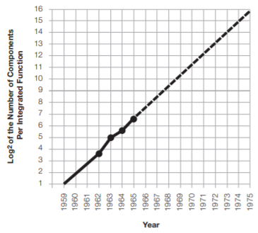
This observation — that the number of components, for minimum cost per component, doubles every year — was dubbed Moore’s Law, and as a prediction for the future, was downgraded by Moore himself in 1975, in a speech titled “Progress in Digital Integrated Electronics” to doubling every two years. Moore’s Law is not a “law” in a scientific sense, like Newton’s laws of motion, or the laws of thermodynamics; instead it is a realistic prediction about the pace of technological advancements in IC density. It is a pace that has become a sort of self-fulfilled prophecy; so many companies in the semiconductor and computer industries have adapted to this rate of advancement, that with today’s complex wafer fabrication processes, they can no longer make technological progress on their own, but instead are dependent on the pace of the group. In some ways, the group of leading-edge technology manufacturers are like the vanguard pack of competitive bicyclists in a race, known as the peloton. According to a 2008 essay by Michael Barry:
The peloton flows with the roads, and we, the cyclists, blindly hope that the flow is not broken. A wall of wheels and bodies means we can never see too far in front, so we trust that the peloton flows around any obstacle in the road like fish in a current.
When in the group, we follow the wheels, looking a few yards ahead, watching other riders to gauge our braking, accelerations and how we maneuver our bikes. Over time, cycling in a peloton becomes instinctual, and our bicycles become extensions of our bodies. When that flow is broken, reaction time is limited and we often crash.
Pat Gelsinger, the present CEO of Intel, stated a different analogy in a 2008 press roundtable — he was a senior vice-president at the time:
According to Gelsinger, Moore’s Law is like driving down a foggy road at night: a headlight allows one to see some distance ahead, but how the driver negotiates the road is up to him. Intel is “on the way to 22[-nm],” Gelsinger said. “We have a good view of what 14[-nm] and [15-nm] will look like, and a good idea of how we’ll break through 10[-nm]. Beyond that, we’re not sure.”
Well… perhaps; the headlight-on-the-foggy-road analogy makes it sound like Moore’s Law is a vision of what’s ahead that helps everyone imagine the future. It’s really a lot more than that: it’s this commitment that allows participants in the semiconductor industry to trust that there is a future. If I had to use a foggy road analogy, I’d change to say it’s more like a extremely nearsighted man driving down a foggy road at night, Mister-Magoo-style, in the forested countryside, while someone else drives ahead of him to make sure the road is clear, pushing the deer and porcupines out of the way.
One approach the industry has used to keep things going is a series of technology “roadmaps”. When everyone follows the roadmap, it all comes together and we get this amazing pace of improvement to keep Moore’s Law going, with transistors getting smaller and smaller, and lower cost per transistor. This does not come easily. The technological work is pipelined, to go as fast as possible, with development just enough in advance of production to make things work reliably and iron out the last few kinks. Wafer fabrication equipment companies and fab process engineers and electronic design automation (EDA) companies and chip designers are all collaborating at the leading edge to use new processes as soon as they are ready. (This hot-off-the-presses stage is called “risk production”.[1])
It’s almost as though there are cars zooming forward on a highway at full speed, and the first cars leading the way are just behind the construction crews that are taking down the traffic cones and the “ROAD CLOSED” signs, which are behind a section of fresh asphalt that has just cooled enough to drive on, which is behind the paving equipment applying asphalt, and the road rollers, and the road graders, and the earth moving equipment, and the surveyors… all moving at full highway speed, to ensure the cars behind them remain unhindered, allowing each driver the oblivious faith needed to keep a foot on the gas pedal.

Source: The Herald-Dispatch, July 2020, photo by Kenny Kemp
Better hurry!
But enough with metaphors — the pace of technology development is dependent on the entire industry, not just one company.
Interlude, 1980s: Crisis and Recovery
The pace of Moore’s Law in the early days just sort of happened organically, as a by-product of the competition between the individual firms of the semiconductor industry. How did this industry-wide coordination come about, then?
In the early 1980s, Japanese companies gained the dominant market share of DRAM suppliers — which I mentioned in Part Two — and the resulting shift to Japan became a sort of slow-motion creeping horror story in the United States semiconductor industry, which had previously dominated most of the semiconductor market. But that wasn’t the end of semiconductor manufacturing in the USA. The DRAM crisis led directly to a number of positive developments.
One was the formation of SEMATECH, an industry consortium of semiconductor manufacturers. As the old SEMATECH website stated:
SEMATECH’s history traces back to 1986, when the idea of launching a bold experiment in industry-government cooperation was conceived to strengthen the U.S. semiconductor industry. The consortium, called SEMATECH (SEmiconductor MAnufacturing TECHnology), was formed in 1987, when 14 U.S.-based semiconductor manufacturers and the U.S. government came together to solve common manufacturing problems by leveraging resources and sharing risks. Austin, Texas, was chosen as the site, and SEMATECH officially began operations in 1988, focused on improving the industry infrastructure, particularly by working with domestic equipment suppliers to improve their capabilities.
By 1994, it had become clear that the U.S. semiconductor industry—both device makers and suppliers—had regained strength and market share; at that time, the SEMATECH Board of Directors voted to seek an end to matching federal funding after 1996, reasoning that the industry had returned to health and should no longer receive government support. SEMATECH continued to serve its membership, and the semiconductor industry at large, through advanced technology development in program areas such as lithography, front end processes, and interconnect, and through its interactions with an increasingly global supplier base on manufacturing challenges.
SEMATECH came in at a critical time and helped the industry organize some basic manufacturing research. Japanese DRAM manufacturers raised the bar on quality, achieving higher yields, and American companies had to react to catch up. Technology roadmapping was also one of SEMATECH’s first organized activities, in 1987.[2] As the semiconductor industry matured, and SEMATECH weaned itself off of government funding, and a number of member companies left in the early 1990s, its importance began to diminish. SEMATECH finally fizzled away around 2015, when Intel and Samsung left — the remnants were merged with SUNY Polytechnic Institute in 2015.
But SEMATECH wasn’t the only consortium that helped U.S. semiconductor firms organize towards improved progress. The Semiconductor Industry Association sponsored a series of cooperative roadmap exercises,[2] with the help of SEMATECH and the Semiconductor Research Corporation, culminating in the National Technology Roadmap for Semiconductors (NTRS) in 1992. This document included specific targets for the semiconductor industry to coordinate together:
The process that the groups followed was to develop the Roadmap “strawman,” or draft, and iterate it with their individual committee members. A revised draft of the Roadmap was issued before the workshop, and the key issues were highlighted for review at the actual workshop.
The charter of the workshop was to evaluate likely progress in key areas relative to expected industry requirements and to identify resources that might best be used to ensure that the industry would have the necessary technology for success in competitive world markets. One underlying assumption of the Semiconductor Technology Roadmap is that it refers to mainstream silicon Complimentary Metal-Oxide Silicon (CMOS) technology and does not include nonsilicon technologies.
…
For the first time, an industry technical roadmapping process prioritized the “cost-to-produce” as a key metric. The cost/cm² was taken as a benchmark metric against which budget targets were developed for the various fab production technologies. For example, lithography was allocated 35 percent of the total, multilevel metal and etch 25 percent, and so forth (see Table 3).
Technical characteristics of note are increasing logic complexity (gates/chip) and chip frequency and decreasing power-supply voltage. These specific characteristics set the vision for requirements for dynamic power for CMOS. They also set in place additional implications for engineering the capabilities to achieve or manage those requirements.
Many organizations have used the Roadmap to set up their own development plans, to prioritize investments, and to act as resource material for discussion of technology trends at various forums, including those of international character. In the United States, one of the most significant results of the workshop was to reinforce a culture of cooperation. The intent to renew the Roadmap on a periodic basis was established.
The 1992 NTRS was followed by another one in 1994:
The success of the 1992 Roadmap prompted the renewal of the Roadmap in 1994. A central assumption of the 1994 process was that Moore’s Law (a 4x increase in complexity every three years) would again extend over the next 15 years. Many experts have challenged this assumption because maintaining the pace of technology and cost reduction is an exceedingly difficult task. Nonetheless, no expectation or algorithm for slowing was agreed upon, and the coordinating committee framed the workshop against extension of Moore’s Law. A 15-year outlook was again taken, this time reaching to 0.07-μm CMOS technology in 2010. A proof of concept exists for low-leakage CMOS transistors near a 0.07-μm gate length. There appears to be no fundamental limit to fabrication of quality 0.07-μm CMOS transistors.
The final NTRS Roadmap occurred in 1997; this was succeeded by an annual series of International Technology Roadmap for Semiconductors from 1998 to 2016, and was subsequently reframed as the International Roadmap for Devices and Systems starting in 2017. NTRS, ITRS, and IRDS have all identified technical challenges needed to continue this pace of development, including transistor design, lithography, packaging, and several other key technologies.
The upshot of all of this is to keep the transistor density increasing.
Moore’s Law keeps marching onwards, and this basically affects us in some combination of four aspects:
-
Chips of the same complexity get smaller, and more of them can fit on a wafer, so in general they cost less. When an IC design is reduced slightly, it’s called a die shrink. Ken Shirriff posted a technical writeup of the 8086 die shrink from 3μm to about 2μm which is worth the read.
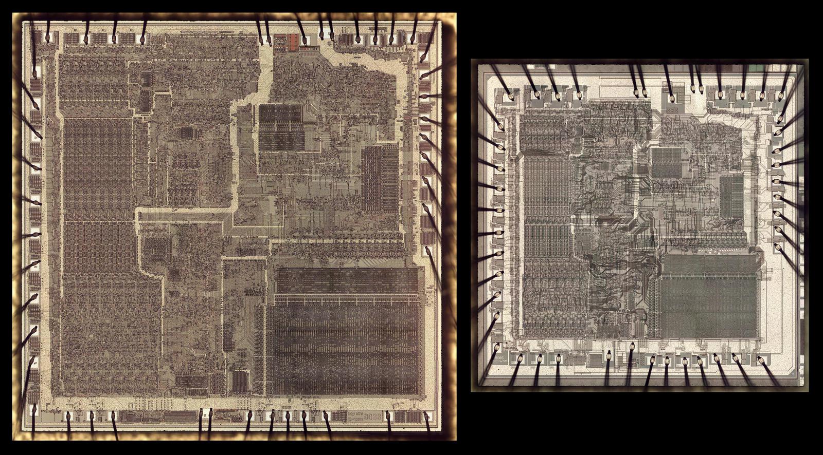
© Ken Shirriff, reproduced with permission
Die shrinks also speed up and/or lower power consumption due to lower parasitic capacitances of the smaller transistors. If you want to get technical, there’s a principle known as Dennard scaling, which maintains the same electric field strength and the same power density per unit area, by reducing the supply voltage for smaller transistor geometries. So we can run smaller feature size chips faster at the same power level, or run them at the same speed with lower power dissipation, or some combination in between.
We can increase the number of transistors to fit more of them in about the same die area. This has been happening for microprocessors for the past 50 years:

Graph by Max Roser, Hannah Ritchie, licensed under CC BY 4.0
These three factors are known as Power-Performance-Area or PPA, and represent tradeoffs in design. If you’re willing to wait to take advantage of the next fabrication process with smaller feature sizes, however, you can improve all of them to some extent.
Benefits, benefits, lots of benefits from Moore’s Law. Yep. And we’ve mentioned how the pace of Moore’s Law is important to coordinate technological investments, and involves industry-wide roadmaps. But a question remains:
How do companies pay for the tremendous cost?
The Depreciation March
I am particularly desirous that there should be no misunderstanding about this work. It constitutes an experiment in a very special and limited direction, and should not be suspected of aiming at achieving anything different from, or anything more than, it actually does achieve.
— Maurice Ravel[3]
Now would be a good time to listen to some music, perhaps Ravel’s Boléro.
Boléro is a rather odd piece of classical music, in that it is one of the most repetitive classical compositions in existence — and yet it is also one of the most famous pieces of the 20th century. It isn’t exactly a march (it has a 3/4 time signature, so more like a waltz) but the pace is metronomic, and as I think of the historical pace of the semiconductor industry, I like to have this music going on in my head. Even though technology makes its way in cycles and bursts of innovation, somehow it is convenient to think of everything moving along in unison.
The semiconductor march of technology has a lot to do with depreciation, which I covered a bit in Part Two. Companies have to account for the expenses they put into capital equipment, and rather than just reporting some big expenditure all at once — which wouldn’t look very good or consistent in a financial statement — they spread it over several years instead. The big expense of semiconductor depreciation is in the wafer fabrication and test equipment, notably lithography machines, and is typically spread over four or five years. The building itself and cooling systems use 10-year or 15-year straight-line depreciation, but tend to be a smaller fraction of the expense. Integrated Circuit Engineering (ICE) estimated that semiconductor equipment comprised 80% of new fab costs in 1996,[4] with the other 20% coming from building construction and other improvements.
And the cost of that fab equipment is increasing. Sometimes this is known as Moore’s Second Law: that the cost of a new fab is rising exponentially. Gordon Moore stated his concern about fab cost in a 1995 article in The Economist:[5]
Perhaps the most daunting problem of all is financial. The expense of building new tools and constructing chip fabrication plants has increased as fast as the power of the chips themselves. “What has come to worry me most recently is the increasing cost,” writes Mr Moore. “This is another exponential.” By 1998 work will have started on the first \$3-billion fabrication plant. However large the potential return on investment, companies will find it hard to raise money for new plants. Smaller firms will give up first, so there are likely to be fewer chip producers—and fewer innovative ideas.
In 1997, ICE cited an estimate of 20% per year increase in the cost to build a leading-edge fab:[6]

Since the late 1990s this appears to have slowed down — in December 2018, the Taiwan News reported the cost of TSMC’s 3nm fab in Tainan as 19.45 billion dollars, which represents “only” a 13.7% annual increase over the roughly \$1.5 billion it cost to build several fabs in 1998[6] — but it’s still a lot of money.
How do they plan to pay for it?
It takes time to build a semiconductor fab and get it up and running productively, so at first it’s not making money, and is just a depreciation expense. Because of this, there is some urgency to make most of the money back in those first few years. In practice, it’s the profits from the previous two technology nodes that is paying for the next-generation fab.
Here’s a graph from a slide that Pat Gelsinger presented at Intel’s 2022 Investor Day:

The x-axis here is time, and the y-axis here is presumably revenue. The \( n \), \( n+1 \), \( n+2 \), \( n+3 \) are generations of process technology.
The idea is that each new process technology goes through different stages of maturity, and at some point, the manufacturer takes it off-line and then sells the equipment to make room for the latest equipment, so the manufacturer’s mix of technology nodes evolves over time.
Finding examples of fabs selling equipment in this manner is tricky — not as straightforward as finding examples of fab sales (of which I mentioned several in Part Two) or fab shutdowns, which make the newspapers, like the 2013 shutdown of Intel’s Fab 17 in Hudson, Massachusetts. This was Intel’s last fab for 200mm wafers, and was closed because, as Intel spokesman Chuck Malloy said at the time, “It’s a good factory. It’s just that there’s no road map for the future.” The transition between 200mm wafer equipment and 300mm wafer equipment is more of a barrier than between technology nodes of the same wafer size; I’m not really sure what that means in practice, but perhaps there are major building systems that need to be upgraded, so a fab that processes 200mm wafers just isn’t cost-effective to upgrade to recent generations of 300mm equipment. The most recent leading-edge fabs that use ASML’s EUV machines require structural design changes in the buildings to accommodate these machines. From a December 2021 article in Protocol describing Intel’s Hillsboro Oregon site:
There are no pillars or support columns inside the plant, which leaves more space for the engineers to work around the tools. Custom-made cranes capable of lifting 10 tons each are built into the ceiling. Intel needs those cranes to move the tools into place, and open the machines up if one needs work or an upgrade. One of the ASML systems Phillips stopped by to demonstrate was undergoing an upgrade, exposing a complex system of hoses, wires and chambers.
“Each [crane] beam can lift 10,000 kilograms, and for some of the lifts you have to bring two of the crane beams over to lift the components in the tool,” Phillips said. “That’s needed to both install them and maintain them; if something deep inside really breaks, you’ll have to lift up the top module, set it on a stand out behind or in front of the tool, then the ASML field-service engineers can get to work.”
Below the EUV tools, Intel built a lower level that contains the transformers, power conditioners, racks of vacuum pumps for hydrogen-abatement equipment systems and racks of power supplies that run the CO2 driver laser. The driver laser shoots the microscopic pieces of tin inside the tool at a rate of 50,000 times a second. Originally made by a laser company called Trumpf for metal cutting, the EUV version combines four of its most powerful designs into a single unit for EUV use, Phillips said.
And an EE News Europe article in April 2022 describing a recent delivery of EUV machines to Intel’s Fab 34 in Leixlip, Ireland: (my emphasis)
The system consists of 100,000 parts, 3,000 cables, 40,000 bolts and more than a mile of hosing. It has taken 18 months of design and construction activity to prepare the Fab 34 building to receive the machine. The building was design [sic] around the scanner, which spans four levels of the factory, from the basement, through to the subfab to the fab. It has an inbuilt crane that extends 3m into the ceiling level. It also needs approximately 700 utility points of connection for its electrical, mechanical, chemical and gas supplies.
It was first transported by 4 Boeing 747 Cargo planes with pieces weighing up to 15 tonnes each. It completed the final part of its journey via road where it was carried by over 35 trucks.
So chances are you’re not going to see old fabs upgraded to use EUV equipment. At any rate, there are reasons that buildings reach the end of their useful life. Fab equipment is a different story, and there is a market for used equipment, but it’s not well-publicized. As a 2009 EE Times article put it:[7]
Mainstream equipment vendors that have divisions focused on selling refurbished gear aren’t anxious to publicize used equipment sales because their marketing efforts are focused on pushing their latest and greatest technology. Few analysts follow the used equipment market, and even those that do acknowledge that it’s difficult to track. But those analysts who do track the market for refurbished equipment forecast that it will rise significantly in 2010 after a down year in 2009.
As evidence that more companies are warming to used equipment buys, Exarcos, Kelley and others point to Texas Instruments Inc.’s October deal to buy a full fab of equipment from Qimonda AG and use it to equip what had been an empty fab shell in Richardson, Texas. While virtually everyone agrees that the TI deal was an unusual circumstance because bankruptcy forced Qimonda to unload an entire fab’s worth of relatively new 300-mm equipment at a huge discount, Exarcos and others say it highlights what has taken place in the past year.
DRAM vendors and others moved swiftly to take capacity offline early this year at the height of the downturn. Other companies were forced by economic reasons to close fabs or file for bankruptcy protection. As a result, there is a glut of used equipment on the market, much of it a lot newer than you would typically find on the market, they say.
Equipment apparently goes through several stages in its life cycle:
- new: high cost (depreciation ongoing) but revenue capture increasing from zero to high revenue
- depreciated: moderate revenue capture with low cost (depreciation complete)
- legacy: low revenue capture with low cost
I prefer to think of it like this, at least as a very rough approximation, without the effects of economic cycles:
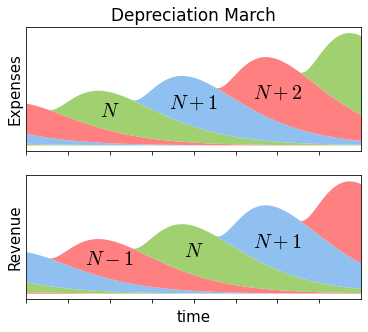
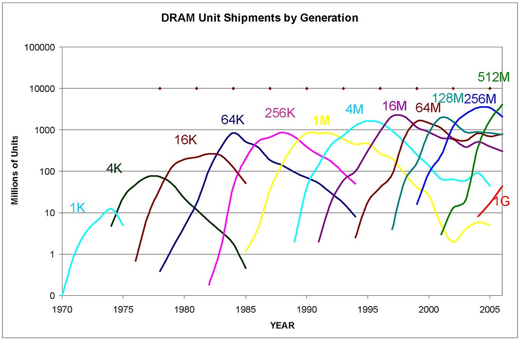
The horizontal tick marks are about a year apart — since 180nm in the late 1990s, the technology nodes have been introduced every two years or so — and the vertical scales are not identical, since revenue has to be larger than expenses to allow some gross margin. Revenue from the next generation \( N+1 \) (“new”) comes in a couple of years after the start of depreciation and development expenses — it takes time to bring up each new process — which are financed by the revenues of generations \( N \) (“new” transitioning to “depreciated”) and \( N-1 \) (“depreciated”). In order to remain profitable, each new generation’s revenue (and expenses) is larger than the previous one. Equipment for depreciated technology nodes brings in income to pay for equipment in new technology nodes, and this new equipment eventually becomes the next set of depreciated equipment three to five years later. Sometime after that, it eventually becomes legacy equipment with low revenue-earning potential, and may be sold to make room for the next round of new equipment. (New, depreciated, legacy, new, depreciated, legacy, one two three, one two three....)
On the expenses side, Scotten Jones of IC Knowledge LLC described it this way in an article, Leading Edge Foundry Wafer Prices,[8] from November 2020:
When a new process comes on-line, depreciation costs are high but then as the equipment becomes fully depreciated the wafer manufacturing costs drops more than in-half. TSMC and other foundries typically do not pass all the cost reduction that occurs when equipment becomes fully depreciated on to the customer, the net result is that gross margins are lower for newer processes and higher for older fully depreciated processes.
Jones also shows a more realistic graph of depreciation expenses in this article — see his Figure 2. Whereas my “expenses” graph looks like a bunch of proportionally-scaled dead whales piled up on each other, his is more irregular and looks like a pile of laundry or misshapen leeches that has toppled over, but otherwise the general characteristics are at least somewhat similar.
On the revenue side:
This behavior makes sense for DRAM, since today’s cutting-edge DRAM chips will become worthless and obsolete in a relatively short time. PC microprocessors have a limited lifetime as well; here’s a graph from Integrated Circuit Engineering (ICE) Corporation’s “Profitability in the Semiconductor Industry”, showing about an 8-10 year life for each Intel processor generation in the 1980s and 1990s, with dominance lasting only about 2-3 years for each generation:[4]

Source: Integrated Circuit Engineering, Profitability in the Semiconductor Industry, Figure 1-25, Product Lifecycle for Intel Processors
So eventually the older legacy nodes fade away. Here’s another example, from a 2009 paper by Byrne, Kovak, and Michaels, graphing different TSMC node revenue:[9]

And a similar graph in cumulative form from Counterpoint Research, showing more recent TSMC earnings data:[10]
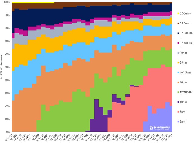
Take a look: 65nm and 40/45nm made up about 40% of TSMC’s revenue in 2013, but now in 2022 they’re on their way out, amounting to barely 10%.
Except something’s not right here.
See if you can figure out what. In the meantime, since these are graphs from TSMC financial statements, we’re going to talk about foundries.
An Introduction to Semiconductor Foundries
It seems odd today, but for the first quarter-century after the invention of the integrated circuit in the late 1950s, semiconductor design and fabrication were tightly coupled, and nearly all semiconductor companies manufactured their own chips. (Today we call that sort of company an integrated device manufacturer or IDM.) I showed this excerpt from New Scientist’s September 9, 1976 issue in Part Two:

At present, Commodore produces the art-work for its calculator chips and subcontracts the chip manufacture to outside plants around the world with spare capacity. The recent purchase of factories in the Far East has enabled it to assemble electronic watch modules by this subcontracting method. But as the up-turn in the economy begins to effect [sic] the consumer electronics industry, less spare capacity is becoming available for this type of subcontracting. When considered along with the additional recent purchase of an LED display manufacturing facility, Commodore now has a completely integrated operation.
Custom chips were a thing in the 1970s, but relied on spare capacity from larger semiconductor companies… and as we saw in Part Two, available semiconductor manufacturing capacity undergoes wild swings every four or five years with the business cycle. Not a particularly attractive place for those on the buying end. Changes began in the late 1970s, with Carver Mead and Lynn Conway’s 1979 book, Introduction to VLSI Systems, that created a more systematic approach to large digital IC designs. Mead had visions of a future where design and fabrication were separated, using Gordon Moore’s term “silicon foundry”. In September 1981, Intel had announced its foundry service; an article in Electronics described Intel’s intentions:
Forging ahead in the foundry business
While one part of Intel knocks on doors for software, another has opened its door to outside chip designers, allowing them to take advantage of its design-automation and integrated-circuit-processing facilities. Though it has been providing the service for six months, the company is just making public the fact that it has set up a silicon foundry in Chandler, Ariz.
Intel is supplying customers with complete sets of design rules for its high-performance MOS and complementary-MOS processes. Also on offer is its scaled-down H-MOS II technology, and even more advanced processes like H-MOS Ill will be added as they become available. Computer-aided-design facilities for circuit layout and simulation will also be provided, as well as services for testing and packaging finished devices.
A manufacturer’s willingness to invite this kind of business usually indicates an overcapacity situation, and Intel’s case is no exception. Indeed, the company says it is setting aside about 10% of its manufacturing capacity for the foundry. However, mixed with this excess capacity is a sincere desire to tap into the foundry business, states manager Peter Jones. “We kicked around the idea when there wasn’t a spare wafer in the industry,” he says of the firm’s long-standing interest in such services.
Referring to more sophisticated customers, Jones explains that “at the system level, their knowledge is greater than ours, so if we don’t process their designs, we’ll lose that share of the business.” The market for the silicon foundry industry could grow from about \$50 million to nearly a half billion dollars by 1985. It is all but certain that Intel will eventually enter the gate-array business as well, perhaps by next year. At present, it seems to be leaning toward a family of C-MOS arrays with high gate count.
— John G. Posa

That same issue of Electronics included an ad from ZyMOS, a small custom chip house, using the term “foundry service”:

John Ferguson summed up the birth of the foundry industry this way, talking about the manufacturing lines at the IDMs:[11]
Occasionally, however, there were times when those manufacturing lines were idle. In Economics 101, we all learned that’s called “excess capacity,” and it’s generally not a good thing. If your machines and staff aren’t doing anything, they’re costing you money. So the semiconductor companies did what any smart business would do—they invented a new industry. They offered up that excess capacity to other companies. At some point, someone realized that by taking advantage of this manufacturing capacity, they could create an IC design company that had no manufacturing facilities at all. This was the start of the “fabless” model of IC design and manufacturing that has evolved into what we have today.
In 1987, someone realized that same model could go the other way as well. The Taiwan Semiconductor Manufacturing Company (TSMC) was introduced as the first “pure-play” foundry — a company that exclusively manufactured ICs for other companies. This separation between design and manufacturing reduced the cost and risk of entering the IC market, and led to a surge in the number of fabless design companies.
TSMC was not the first foundry — as the September 1981 Intel announcement and ZyMOS ad illustrates. Foundries were going to happen, one way or another. But focusing solely on wafer fabrication for customers — not as a side business, and not in conjunction with IC design services — was TSMC’s key innovation, and the “someone” who realized it could work was Morris Chang, founder of Taiwan Semiconductor Manufacturing Company in 1987.
Chang had spent 25 years at Texas Instruments, and then, after a yearlong stint as president and chief operating officer of General Instrument, left to head Taiwan’s Industrial Technology Research Institute (ITRI). ITRI had played a pivotal role in the birth of Taiwan’s semiconductor industry in March 1976, when one of ITRI’s subgroups, the Electronics Research Service Organisation (ERSO), struck a technology transfer agreement with RCA, to license a 7-micron CMOS process and receive training and support. RCA was a technology powerhouse in the middle decades of the 20th century, under the leadership of David Sarnoff, and had pioneered the first commercial CMOS ICs in the late 1960s. But as Sarnoff grew older, his son Robert took his place as RCA’s president and then as CEO, and the younger Sarnoff more or less fumbled the company’s technical lead in semiconductors in the early 1970s, chasing consumer electronics (television sets, VCRs, etc. — my family upgraded from a Zenith black-and-white vacuum-tube TV to an RCA color transistor TV in 1980) and conglomerate pipe dreams; RCA missed out on a chance to hone its strengths in semiconductor design and fabrication and to make CMOS rule the world. Meanwhile, NMOS, not CMOS, dominated the nascent microprocessor and DRAM markets, at least in the 1970s. RCA did manage to get at least some income from licensing CMOS to companies like Seiko. The ITRI/ERSO agreement came amid RCA’s swan song in semiconductors:[12]
ITRI had accomplished the introduction of semiconductor technology to Taiwan. Of course Taiwan was still far from catching up with advanced nations but the main goal was to learn more about semiconductor technology, and to accumulate knowledge. For this goal, a pilot plant, with design, manufacturing and testing capabilities had been built, and was geared towards producing simple semiconductors. As noted, RCA had developed the first CMOS integrated circuits, but CMOS was at the time not a widespread technology. RCA was actually about to withdraw from the semiconductor industry and the licensing deal with ITRI was an opportunity to squeeze some last income from a mature technology. The 7.0 micron CMOS was mature, and far behind the worlds leading LSI 2.0 micron circuit designs, nonetheless for ERSO this was a way of gaining access to the world of semiconductors. In retrospect, the licensing of CMOS technology proved to be a wise choice. First of all ITRI did not have to directly compete with established producers on a global market. Second the market share of CMOS was relatively small at the end of the 1970s, but started to expand rapidly afterwards to become the most used technology in IC design today. After RCA withdrew from the semiconductor industry in the early 1980s, ITRI also inherited the intellectual property portfolio from RCA that had been related to CMOS technology (Mathews and Cho, 2000).
(The irony, of course, is that eventually CMOS did come to rule the semiconductor world, without RCA in it.)
Chang had not been at the helm of ITRI long when the Taiwan government asked him to start a semiconductor firm, according to an article in IEEE Spectrum about Chang’s founding of TSMC:[13]
Taking on the semiconductor behemoths head-to-head was out of the question. Chang considered Taiwan’s strengths and weaknesses as well as his own. After weeks of contemplation he came up with what he calls the “pure play” foundry model.
In the mid-’80s there were approximately 50 companies in the world that were what we now call fabless semiconductor companies. The special-purpose chips they designed were fabricated by big semiconductor companies like Fujitsu, IBM, NEC, TI, or Toshiba. Those big firms drove tough bargains, often insisting that the design be transferred as part of the contract; if a product proved successful, the big company could then come out with competing chips under its own label. And the smaller firms were always second-class citizens; their chips ran only when the dominant companies had excess capacity.
But, Chang thought, what if these small design firms could contract with a manufacturer that didn’t make any of its own chips — meaning that it wouldn’t compete with smaller firms or bump them to the back of the line? And he realized that this pure-play foundry would mean that Taiwan’s weaknesses in design and marketing wouldn’t matter, while its traditional strengths in manufacturing would give it an edge.
TSMC opened for business in February 1987 with \$220 million in capital—half from the government, half raised from outside investors. Its first customers were big companies like Intel, Motorola, and TI, which were happy to hand over to TSMC the manufacture of products that used out-of-date technology but were still in some demand. That way, the companies wouldn’t have to take up their own valuable fab capacity making these chips and would face little harm to their reputation or overall business if TSMC somehow failed to deliver.
At the time, TSMC was several generations behind the leading-edge CMOS processes. Now, of course, TSMC is the leading semiconductor foundry in the world, with over 50% market share among the foundries (Samsung is a not-so-close second) and is among the only companies left that manufacture the most advanced technology nodes. Foundries like TSMC and UMC are more or less the Taiwanese equivalent to Swiss banks: neutral parties facilitating business from all over the world.
The fabless industry is no longer just a place for relatively small semiconductor companies who don’t want to own their own wafer fabs. Today’s foundry customers include technology giants such as Apple, Nvidia, and Qualcomm. Most of the former IDMs, including all of the major microcontroller manufacturers, are now in the “fab-lite” category, relying on their own fabs for cost-effective manufacturing of larger technology nodes, but outsourcing more advanced manufacturing processes to TSMC / UMC / SMIC / etc. Even Intel uses external foundries like TSMC, although it’s trying to keep the focus on its own leading-edge manufacturing.
Half of TSMC’s revenue now comes from technology nodes 7nm and smaller. Which brings us back to that Counterpoint Research graph.
Not Fade Away
It’s mesmerizing, isn’t it? What strikes me is the stationarity: the distribution of revenue at TSMC is more or less the same no matter what year it is. In 2013 the three leading-edge processes (28nm, 40/45nm, and 65nm) make up about 60-65% of revenue. In 2018 the three leading-edge processes (10nm, 12/16/20nm, and 28nm) make up about 60-65% of revenue. In 2022 the three leading-edge processes (5nm, 7nm, 16nm — TSMC has settled on 16nm, according to its quarterly reports) make up about 60-65% of revenue.
Which is what, presumably, TSMC and the semiconductor industry want. Stability in motion. A perpetual leading edge; just jump on for a ride anytime you like. Don’t worry, we’ll keep Moore’s Law going.
I was researching the economic impacts and implications of Moore’s Law in October 2021, searching for answers. How does this work? Some of it was unsettling. I mean Moore’s Law can’t go on forever, can it? Sooner or later you run into atomic scale and then what? But apparently we’ve still got a ways to go, at least on the technological front. The metaphor I had in mind then wasn’t a peloton, or Mister Magoo driving on a foggy road, or a bunch of cars driving on a just-paved-in-time highway, or a Depreciation March — it was more like a sleighride careening downhill just barely in control, or like Calvin and Hobbes on a toboggan, or the protagonists in Green Eggs and Ham as they ride on a train down questionably-engineered tracks, the train’s passengers relaxing serenely all the while. (We never do find out the name of the guy who says he doesn’t like green eggs and ham.) Anyway, everything’s stable as long as the ride goes on downhill, but what happens at the end?
That part I can’t answer.
The economic implications of Moore’s Law in recent years, on the other hand, are out there, but some of them are subtle; you just have to look around a bit. One is the rising costs of IC development. Here’s a graph from Handel Jones at IBS, which was included in a 2018 article titled Big Trouble At 3nm:[14]

Yikes! Half a billion dollars to design one chip using 5nm technology is some serious spending. What isn’t clear from graphs like these, however, are the conditions. Is it a die of a given area, say, 6mm x 6mm? If so, the transistor counts are going up along with the complexity, so sure, I would expect the costs to rise. But what happens if I have a chip design that’s going to need 10 million transistors, regardless of whether it’s 28nm or 65nm or 130nm… how does the design cost change with the technology node?
I can’t answer that question, either.
About this time (October 2021) I ran across a series of publications from McKinsey & Company, titled (what else) McKinsey on Semiconductors. Which are good reads; just realize that instead of coming from the technological angle, they’re coming from the management-consultant angle: custom answers for \$\$\$\$; don’t bother asking the questions, since they will tell you the questions you should have asked. Anyway here’s a graph from McKinsey on Semiconductors 2011 that made me do a double-take:

Huh. Leading-edge nodes are only a small share of foundry volume.
The leading edge is where all the money is going. Lots of expense but lots of revenue, even if it’s not a large share of capacity. Today manufacturing a 7-nanometer wafer full of finished chips might cost ten times what a 180-nanometer wafer costs. But that’s because of the cost of depreciation. Once the 7-nanometer equipment has been paid for, the cost of a finished wafer will come down, and then 5-nanometer and 3-nanometer will make up the bulk of the revenue. New, depreciated, legacy, new, depreciated, legacy.... Billions of dollars is on the line from the foundries, from the EDA companies, from the semiconductor equipment companies, and the only way the economics are going to work so well is if they are reasonably stable and predictable: yesterday’s advanced nodes pay for tomorrow’s even more advanced nodes, while yesterday’s advanced nodes become mature nodes, and the capacity of those mature nodes is there for everyone to use to keep the cost down. There have been some hiccups; after 28-nanometer, most of the foundries took a little longer than expected to get to FinFETs, and EUV finally arrived in time to make a big difference, like a star actor bursting on-stage just in time for Act IV of the play. But overall, Moore’s Law has kept right on going.
Still: leading-edge nodes are only a small share of foundry volume. So all the trailing-edge mature legacy nodes are still there; they bring in some revenue, but not as much as the leading edge. And they don’t go away!
That was the part that made me do the double-take. Yes, if you look at things in relative terms, the older technology nodes make up a smaller percentage of foundry capacity than they used to. But the foundry capacity of mature nodes is still there, pumping out new chips year after year. With the chip shortage going on, maybe there’s a perception that the industry has been bringing old technology off-line intentionally, or that adverse events like COVID-19 have reduced available capacity — this is not the case! The capacity has been maintained all this time, but the demand has gone up and we’ve bumped up pretty hard against a supply limitation.
The McKinsey graph is from 2011. I couldn’t find any similar data on foundry capacity that is more recent, but TSMC does publish its financial results every quarter, and they break down their revenue by technology node — I’m assuming the Counterpoint Research graph just used that data — so if you’re willing to go to the trouble to visit TSMC’s website, you can analyze their financial data yourself. Let’s take a look:
Fun With Foundry Financial Figures
I went back over the last 20 years and here’s my graph:

TSMC itself reports revenue breakdown by node as a percentage of total revenue, not in dollars — but it also reports total revenue in New Taiwan dollars, so you can just multiply the two together to get revenue in absolute terms, at least within the granularity of around 1% of the total revenue.[15] Here’s an example from the TSMC 2Q22 Management Report:
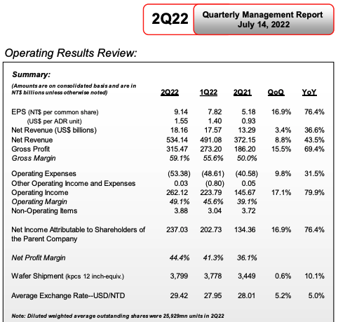
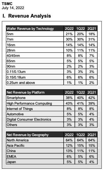
Some of the node groups on my graph, which I think of as “buckets”, are a little weird (16/20nm together, and 110/130nm and 150/180nm) but that’s just the way TSMC has lumped them together during most of their history, so to get some consistency, when I looked at the older results I used the same buckets — in other words, back in 2003 when 150nm and 180nm were reported separately I just added those together. Or today, when TSMC just reports 16nm, not 16/20nm — I presume 20nm is dead? — I still applied it to the same 16/20nm bucket.
Anyway it’s remarkable how level these revenue lines are. (Well, at least prior to the chip shortage.) There’s a little blip around the first quarter of 2009 — that’s the 2008 financial crisis kicking in — and in the past year or so, an uptick across-the-board, presumably due to the increased demand of the chip shortage and TSMC’s price increases. Oh, and there was 10nm’s untimely death; now TSMC just reports 16nm and 7nm. But look at 150/180nm. Twenty years and it keeps on going! The same, more or less, with 65nm and 40nm. The 90nm and 110/130nm nodes have decreased since their introduction, but otherwise they’re still there; 28nm and 16nm have come down slightly also.
What would be really interesting is to see the number of wafers manufactured for each node, rather than the revenue, since presumably the cost per wafer decreased after the first few years of production. But that’s proprietary information and I don’t expect TSMC to be very forthcoming.
The graph from Intel’s 2022 Investor Day that I cited earlier is actually from a slide that contains several graphs:

Intel’s message, apparently, is that they want to stop throwing away the old equipment and keep it in use, the way TSMC has done, and squeeze out those extra drops of revenue at the trailing edge — well, at least that’s what I read into it.
Leading-edge nodes are only a small share of foundry volume. And trailing-edge nodes keep on living, bringing in revenue. (Despite rumors to the contrary.)
For TSMC, this isn’t just an accidental phenomenon visible to the careful observer; it’s a conscious decision. Dr. Cheng-Ming Lin has been quoted several times in TSMC’s recent Technology Symposiums of the company’s deliberate decision to keep their processes going.
- In 2018: “We never shut down a fab. We returned a rented fab to the government once.”[16]
- In 2019: “Our commitment to legacy processes is unwavering. We have never closed a fab or shut down a process technology.”[17]
Paul McLellan commented on this in 2019:[18]
The strategy is to run mainline digital when a fab is new, and then find more lines of business to run in it as the volume of digital wafers moves to the next fab over the following years.
The fabless/foundry business model that TSMC pioneered has several advantages over what we just called the “semiconductor business model” and now say “integrated device manufacturer” or IDM. In the old model, where a semiconductor company had fabs, the whole mentality was to fill the fab exactly with lines of business. The company needed just the right amount of business to fill its fabs: not enough, and the excess depreciation was a financial burden, too much and they were on allocation and turning business away. When a fab got too far off the leading edge, there might not be enough business to run in it, and the fab would be closed. Or, in the days when many companies had both memory and logic businesses, they would run memory and then convert the fab to logic, and then eventually close it.
TSMC finds new lines of specialty technologies, finds new customers, and keeps the fabs going. Things like CMOS image sensors (CIS) or MEMS (micro-electrical-mechanical-systems such as pressure sensors). Adding new options to non-leading edge processes such as novel non-volatile memories.
It’s almost as if Henry Ford’s original factory for the Model T was still running, but now making turbine blades for the aerospace industry.
TSMC isn’t the only foundry with this strategy — although it’s so large that sometimes I just think of “TSMC” and “foundries” interchangeably. United Microelectronics Corporation, also located in Taiwan (UMC was ITRI’s first commercial spinoff in 1980, although didn’t get into the pure-play foundry business until 1995), is the third-largest semiconductor foundry in market share after TSMC and Samsung, and it also posts similar information in its quarterly financials:

Plenty of mature nodes in the works, and although I haven’t crunched the numbers on UMC’s financials as carefully as TSMC’s, here’s a similar graph for the second quarter of each year between 2001 and 2022:

UMC’s revenue data has a little more fluctuation than TSMC — probably because UMC is a smaller foundry; the law of large numbers expects more variability in companies with fewer customers — but it’s the same general pattern.
UMC publishes a few tidbits in its earnings reports that TSMC does not choose to share with us, all of which are interesting and lend a little bit more of a glimpse into the world of foundries:
- IDM revenue share
- utilization
- capacity by fab
The IDM revenue share is the percentage of revenue that comes from customers who have their own fabs (remember: IDM = integrated device manufacturer) but choose to outsource some of their wafer production to UMC. Because of this, the term “fab-lite” is more apt than IDM. At any rate, look at the fluctuation:

In the third quarter of 2006 this hit an all-time high of 44%. This was about the time of a very strong PC market that caught semiconductor manufacturers off guard[19] and was the main catalyst for the 2006-2009 DRAM crisis, which I mentioned in Part Two. UMC’s quarterly report states[20]
The percentage of revenue from fabless customers decreased to 56% in 3Q06 from 63% in 2Q06 as several Asian fabless customers adjusted their inventory levels, although demand from IDM customers remained strong.
IDM revenue has made up a much lower fraction of UMC’s business in the past ten years or so.
Utilization measures how much of the available capacity is actually in use; UMC defines this as “Quarterly Wafer Out / Quarterly Capacity” (wafer shipments divided by wafer capacity)

Aside from the economic downturns in 2001 and 2008, UMC has managed to keep fab utilization high. In recent quarters, wafer shipments have been above wafer capacity; because of the urgency (and profitability) of getting product to customers during a time of shortage, the fabs have managed to squeak out a little bit more than their maximum capacity. (It is not at all obvious that it would be possible to go above 100% utilization; more on this in Part Five.)
UMC also states their wafer capacity by fab, with tables like these:

It’s not quite as informative as a breakdown of capacity by technology node, but we can graph this in 8” (200mm) equivalent capacity:

UMC’s Fab 12A is a huge catch-all fab complex (130nm – 14nm at present) with construction in phases, projected to eventually cover eight phases when fully built out. According to UMC’s website:
Fab 12A in Tainan, Taiwan has been in volume production for customer products since 2002 and is currently manufacturing 14 and 28nm products. The multi-phase complex is actually three separate fabs, consisting of Phases 1&2, 3&4, and 5&6. Fab 12A’s total production capacity is currently over 87,000 wafers per month.
It would be interesting to see what their capacity is per node.
Or, perhaps more interesting: how does the average customer price per unit area of silicon depend on the technology node? Neither UMC nor TSMC publish how many wafers they make on each technology node. The best I could do was estimate from per-fab capacity data (TSMC published this from 2006 to 2014) that in 2012 TSMC’s 300mm fabs probably earned around 50% more per unit die area, on average, than the 200mm fabs; this average pricing premium increased to around 60% in 2013 and to around 85% in 2014, as more advanced nodes came online. Pricing at the leading edge is likely a lot higher, which skews revenue in favor of the latest nodes, even though (as I’ve now said several times) leading-edge nodes are only a small share of foundry volume.
TSMC did address this issue (more advanced nodes cost more) in its 2006 annual report (my emphasis):
Technology Migration. Since our establishment, we have regularly developed and made available to our customers manufacturing capabilities for wafers with increasingly higher circuit resolutions. Wafers designed with higher circuit resolutions can either yield a greater number of dies per wafer or allow these dies to be able to integrate more functionality and run faster in application. As a consequence, higher circuit resolution wafers generally sell for a higher price than those with lower resolutions. In addition, we began in November 2001 offering our customers production of 300mm wafers which can produce a greater number of dies than 200mm wafers. Advanced technology wafers have accounted for an increasingly larger portion of our sales since their introduction as the demand for advanced technology wafers has increased. Because of their higher selling price, advanced technology wafers account for a larger pro rata portion of our sales revenue as compared to their pro rata share of unit sales volume. The higher selling prices of semiconductors with higher circuit resolutions usually offset the higher production costs associated with these semiconductors once an appropriate economy of scale is reached. Although mainly dictated by supply and demand, prices for wafers of a given level of technology typically decline over the technology’s life cycle. Therefore, we must continue to offer additional services and to develop and successfully implement increasingly sophisticated technological capabilities to maintain our competitive strength.
But there’s not any quantitative information here… is a 28nm wafer 1.6× the cost per area of a 180nm wafer? or 5× the cost per area?
Oh, if we could only get some more specific information, some better quantitative insight into the variation in price and operating cost and profitability for the different foundry node geometries.... Presumably this is highly proprietary business information for any fab owner, foundry or not — but I do wish that after some period of time (10 years? 15 years?) these companies would publish historical information for us to better understand how the industry works, without significantly impairing any competitive business advantage.
There are certainly some unofficial outside estimates of cost per wafer; I’ll discuss one such reputable estimate in a later section on cost modeling. And there are periodic news rumors that can lead to a less-reputable estimate: for example, DigiTimes mentioned in a March 2022 article that TSMC’s 5nm wafer shipments were around 120,000 wafers per month and would be increasing to 150,000 wafers per month by the third quarter of 2022. If this is accurate, 120KWPM (360K wafers per quarter) represents nearly 10% of TSMC’s first-quarter 2022 shipments (3778K twelve-inch equivalent) but TSMC reported 5nm made up 20% of 2022Q1 revenue (NT\$86.292 billion in 2022Q1’s Consolidated Financial Statements ≈ US\$3 billion, which works out to about \$8300 on average per 5nm wafer; TSMC’s total wafer revenue for 2022Q1 was NT\$438.64 billion ≈ US\$14.5 billion → divide by the 3778K 12” equivalent wafers shipped and we get US\$3800 per 12” wafer on average across all nodes) so 5nm earns an outsized share of revenue relative to the older nodes.
At any rate:
Leading-edge nodes are only a small share of foundry volume. And trailing-edge nodes keep on living, bringing in revenue.
Now, the big question to ask yourself is: with this sort of fab behavior — nothing old disappears, while new nodes keep on adding to capacity, becoming more profitable once equipment depreciation is completed — how have the foundries’ business models impacted the chip shortage?
Notes
[1] Ron Wilson, TSMC risk production: what does it mean for 28nm?, EDN, Aug 26 2009.
[2] W. J. Spencer and T. E. Seidel, International Technology Roadmaps: The U.S. Semiconductor Experience (Chapter 11), Productivity and Cyclicality in Semiconductors: Trends, Implications, and Questions: Report of a Symposium. Washington, DC: The National Academies Press, 2004.
[3] Michel-Dimitri Calvocoressi, M. Ravel Discusses His Own Work, Daily Telegraph, Jul 11 1931. Reprinted in A Ravel reader: correspondence, articles, interviews, 2003.
[4] Integrated Circuit Engineering Corporation, Cost Effective IC Manufacturing 1998-1999: Profitability in the Semiconductor Industry, 1997.
[5] The End of the Line, The Economist, vol. 336, no. 7923, Jul 15 1995.
[6] Eric Bogatin, Roadmaps of Packaging Technology: Driving Forces on Packaging: the IC, Integrated Circuit Engineering Corporation, 1997.
[7] Dylan McGrath, Analysis: More buyers seen for used fab tools, EE Times, Dec 22 2009.
[8] Scotten Jones, Leading Edge Foundry Wafer Prices, semiwiki.com, Nov 6 2020.
[9] David M. Byrne, Brian K. Kovak, Ryan Michaels, Offshoring and Price Measurement in the Semiconductor Industry, Measurement Issues Arising from the Growth of Globalization (conference), W.E. Upjohn Institute for Employment Research, Oct 30 2009.
[10] Leo Wong, High Performance Computing Surpasses Smartphones as TSMC’s Highest Revenue Earner for Q1 2022, Gizmochina, May 7 2022.
[11] John Ferguson, The Process Design Kit: Protecting Design Know-How, Semiconductor Engineering, Nov 8 2018.
[12] Ying Shih, The role of public policy in the formation of a business network, Centre for East and South-East Asian Studies Lund University, Sweden, 2010.
[13] Tekla S. Perry, Morris Chang: Foundry Father, IEEE Spectrum, Apr 19 2011.
[14] Mark LaPedus, Big Trouble At 3nm, Semiconductor Engineering, Jun 21 2018.
[15] Actually, if you want more precise numbers for revenue by process technology, you can look for TSMC’s consolidated financial statements as reviewed by independent auditors. From the 2022 Q2 consolidated financial statement:

I ran across these recently, after I had already typed in all the revenue percentage numbers from the past 20 years of quarterly management reports.
[16] Paul McLellan, TSMC’s Fab Plans, and More, Cadence Breakfast Bytes, May 7 2018.
[17] Tom Dillinger, 2019 TSMC Technology Symposium Review Part I, SemiWiki.com, Apr 30 2019.
[18] Paul McLellan, TSMC: Specialty Technologies, Cadence Breakfast Bytes, May 2 2019.
[19] Jeho Lee, The Chicken Game and the Amplified Semiconductor Cycle: The Evolution of the DRAM Industry from 2006 to 2014, Seoul Journal of Business, June 2015.
[20] United Microelectronics Corporation, 3Q 2006 Report, Oct 25 2006.
Supply Chain Games 2018: If I Knew You Were Comin’ I’d’ve Baked a Cake
Oh, I don’t know where you came from
‘Cause I don’t know where you’ve been
But it really doesn’t matter
Grab a chair and fill your platter
And dig, dig, dig right in— Al Hoffman, Bob Merrill, and Clem Watts, 1950
While you think about foundries and their business models in the back of your mind, let’s talk about today’s game.
Here we leave the 8-bit games of the 1980s behind; today’s computer games are behemoths in comparison. This one is called Supply Chain Idle and it runs in a web browser on a framework called Unity, probably using thousands of times as much memory and CPU power as Lemonade Stand and M.U.L.E. did on the 6502 and 6510 processors.
Thanks, Moore’s Law!
At any rate:
In the game of Supply Chain Idle, you are in charge of a town called Beginner Town. It has 20 industrial plots of land in a 5×4 grid interconnected by roads. You start out with four dollars in your pocket, and can buy apple farms and stores, each for a dollar. That’s enough for two apple farms and two stores. If you put them on the map and connect the apple farms and the stores, then the apple farms start making apples and trucks transport those apples to the stores to be sold.

At first, the rate of apple production is one apple every four seconds, which you can sell at the store for the lofty price of ten cents apiece, in batches of ten apples every five seconds.
With two apple farms and two stores:
- We can produce up to two apples every four seconds = 0.5 apples per second.
- We can sell up to 20 apples every five seconds = 4.0 apples per second
The stores can sell them faster than you can make them, so that means the apple farms are the bottleneck, and at ten cents each, we’re making five cents a second. After 20 seconds, we have another dollar, and can buy another apple farm or store.
We could fill the map with 10 apples and 10 stores. Apple farms would still be the bottleneck, but now we’d be making 25 cents a second.

Or we could be a bit smarter, and realize that with 18 apple farms and 2 stores:
- the farms produce 18 apples every 4 seconds = 4.5 apples per second
- the two stores could sell up to 20 apples / 5 seconds = 4.0 apples per second
In this case, the stores are the slight bottleneck, but now we can make money faster, selling apples at a total of \$0.40/second.

That’s still not very much. (Well, actually, it’s a lot. 40 cents a second = \$24 a minute, \$1440 an hour, \$34560 a day, or \$12.6 million a year. In real life, I’d take it and retire. But in the game, it isn’t very much.) To make more money in Supply Chain Idle, there are a number of methods:
-
Complete achievements. These are milestones like “sell 100 apples” or “get \$100 cash on hand”. Some of the achievements will raise prices by 1% or lower production times by 1%, either of which will increase the rate at which you make money.
-
Shop at the store and spend idle coins on speedups. If you have 100 idle coins, you can triple all prices. You can get idle coins by spending real money (PLEASE DON’T!) or by earning enough achievements… though that takes a long time. This is good for later in the game; save your idle coins for the super speed (10× production rate for 300 coins) if you can.
-
Build more resource producers. We’re already maxed out using all 20 spaces, so that won’t help.
-
Balance production with the rate at which it can be consumed and sold. Already done that for apples — but this is a big part of the game. In case you want to change your mind, Supply Chain Idle lets you sell back resource producers and stores for a full refund. (Try that in real life: good luck.)
-
Upgrade! Just like the Kittens Game, upgrading is a big part of Supply Chain Idle, and there are five ways to upgrade. Resource producers have productivity, speed, and quality levels, while stores have marketing and speed levels.
a. Increase productivity. Each of your resource producers has a productivity level, which increases the amount produced in each batch. For example, to go from Level 0 to Level 1 productivity in apples, you spend \$6 and go from 1 apple in 4 seconds (0.250 apples/second) to 2 apples in 6 seconds (0.333 apples/second), which is a 33.3% speedup.
b. Increase resource producer speed. This increases the speed each batch is produced. To go from Level 0 to Level 1 speed in apples, you spend \$5 and go from 1 apple in 4 seconds to 1 apple in 2 seconds, which is a 100% speedup.
c. Increase resource producer quality. This raises the price you can get from the store. To go from Level 0 to Level 1 quality in apples, the price increases from 10 cents to 13 cents each, which is a 30% price increase.
d. Increase marketing. This lets the stores sell more at a time; to go from Level 0 to Level 1 marketing, the store goes from a batch of 10 in 5 seconds (= 2/second) to a batch of 20 in 7.5 seconds (= 2.666/second), a 33.3% speedup.
e. Increase store speed. This lets the store sell each batch faster; to go from Level 0 to Level 1 speed, the store goes from a batch of 10 in 5 seconds to a batch of 10 in 2.5 seconds, a 100% speedup.
Like selling the resource producers and stores, you can also downgrade any upgrade and get a full refund.
-
Make a new product! Once you sell apples, and have \$100 on hand, you can buy a sugar cane farm. Sugar cane can be produced starting at a batch of 12 in 2 seconds, with a store price of \$0.303… this is \$1.818 per second, much better than the \$0.025 per second you’ll get at the beginning from apples.

Sugar cane is produced in much higher quantities per second than apples, so the balance between sugar cane farms and stores is different; at one point it looked like I needed about 3 stores for each sugar cane farm. This can change with resource producer or store upgrades, but at some point the cost of the upgrades becomes too high and you’re stuck trying to figure out how to make do with the money you have.
Each time you sell the first unit of a new product, it unlocks the next product. After sugar cane is sugar, which shows one more game dynamic, namely that there are raw resource producers (like apples and sugar cane farms) where there are no production inputs, and resource processors like sugar mills, which need inputs taken from other resource producers. Sugar production needs sugar cane as an input, so the supply chain here goes sugar cane → sugar → \$\$\$. At the time I started sugar production in this game, a sugar mill cost \$20,000 and turned 1700 units of sugar cane into one unit of sugar in about 10 seconds, which I could sell for the price of \$6072 = \$607/second.

The game warns you with a little colored dot in the upper right hand corner of a grid square if the supply chain is not well-balanced in the store or a downstream production step. Stores show orange or red dots if they can’t keep up with the rate of product being added. Resource processors (like sugar mills) show orange or red dots if they can’t get enough inputs to keep producing outputs and have to wait for the inputs to arrive.
The supply chain shown above (one sugar mill supplied from one sugar cane farm) is poorly balanced; here’s a better one with one sugar mill and 18 sugar cane farms, producing \$841/s:
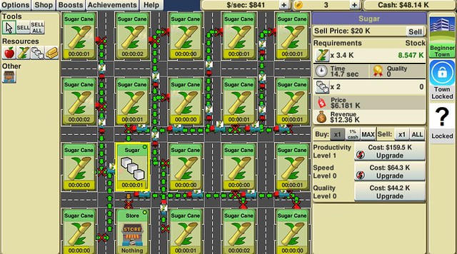
With two sugar mills each supplied by 8 sugar cane farms, I can get \$1266/s even though the sugar mills are a little undersupplied (the color indicator is yellow rather than green):

The upgrade prices go up roughly exponentially, and by the time you have enough money to buy the next resource producer, it’s usually worth it to switch right away. You’ll note that there are no apple farms in the last few images, and as soon as sugar mills are in the mix, it’s no longer worth selling the sugar cane directly to the store — instead, all the sugar cane should be provided as input to the sugar mills.
Next comes lumber mills — \$7 million each; not sure how they churn out lumber without any input from trees… but that’s the way it goes in Beginner Town! — and after that, paper carton plants, at \$3 billion apiece. Sometimes the mills are the bottleneck and sometimes stores are the bottleneck; the game can shift very quickly.
After the first few resource producers, a lot of the game time involves waiting — which is why it is an idle game rather than something that should be actively played — and the big question becomes: what upgrade should be done next? I don’t have a good general strategy for this; it just takes some effort to figure out what upgrade gives the biggest bang for the buck. Quality upgrades are worth pursuing, even the lower ones which make less of a difference: for example, upgrading paper carton plant quality will make more of a difference than upgrading the lumber mill quality in the final price of paper cartons, but both are still worth doing.
If you hover over any of the upgrade buttons, the game will tell you what effect it will have in advance. For example here I’ve upgraded the various factories in Beginner Town so that I’m making \$5.283 billion per second, and the least expensive upgrade will be a quality upgrade for the paper carton plant, which will bump up the price of paper cartons by 30% — so now I can earn \$6.867 billion per second — but that upgrade will cost me \$303.1 billion. I have \$191.2 billion in cash now, so that will take me another 21 seconds to afford the upgrade, and I’ll need to spend all my remaining cash. Is it worth it?

Well, the next major hurdle in the game is buying an apple juice factory for \$6 trillion — I kid you not — so if I don’t do the quality upgrade, it will take me 1100 seconds, or about 18 minutes. If I do the quality upgrade, it will take me 21 seconds to afford the upgrade, and another 14 minutes to earn the \$6 trillion. Definitely worth the upgrade.
If you want to see this graphically, here it is; there’s a breakeven point at about 3.5 minutes where the upgrade gets us further.
import numpy as np
import matplotlib.pyplot as plt
%matplotlib inline

R1 = 5.283e9              # production rate before upgrade
C0 = 191.2e9              # starting cash
U2 = 303.1e9              # cost to upgrade quality
Ctarget = 6e12            # target cost
R2 = R1 * (61.68/47.45)   # production rate after upgrade
tu = (U2-C0)/R1
t1 = (Ctarget-C0)/R1
t2 = Ctarget/R2
fig = plt.figure(figsize=(8,5))
ax = fig.add_subplot(1,1,1)
ax.plot(np.array([0, tu, tu, tu+t2])/60,
        np.array([C0, U2, 0, Ctarget])/1e9,
        '-',label='upgrade')
ax.plot(np.array([0, t1])/60,
        np.array([C0, Ctarget])/1e9,'--',label='no upgrade')
ax.grid(True)
ax.set_xlabel('Time (minutes)')
ax.set_ylabel('Available cash (\$B)')
ax.set_xticks(np.arange(0,20,2))
ax.set_xlim(0,20)
ax.legend();
(This game suffers from the “–illions inflation” of many idle games, something I mentioned in Zebras Hate You For No Reason. You just have to ignore the implausibility if you want to have fun.)
Anyway, after a short time, I do have the \$6T to afford an apple juice factory, and I start building. This is the first complex supply chain:
- apple juice ← (apples, sugar, paper carton)
- sugar ← sugar cane
- paper carton ← lumber

The setup I have shown here is not very good, and the apple juice factory has a red dot, which means I’m not utilizing the factory very well. Maximizing profit in this game is all about balancing the supply chain, and we’re not. The “Stock+Supply” panel tells us a couple of things here:
-
Each supply input for apple juice has an ideal rate to keep the apple juice factory at full utilization. The game shows you the supply rate of each input relative to full utilization, as a percentage. Right now we’re providing 225% of that ideal rate in paper cartons, 30% of the ideal rate in sugar, and 19% of the ideal rate in apples. That leaves the utilitization of the apple factory at only 19%, and means that it’s waiting 81% of the time. Apples are the bottleneck, so if we want more apple juice, we need to increase apple production. Supply rate percentages are shown in red if less than 100%, green otherwise.
-
With current production rates, the game recommends supplying each apple juice factory with 6 apple farms, 3 sugar mills, and 1/5 of a paper carton plant. (Another way of thinking about it: a paper carton plant can supply 5 apple juice factories.)
-
The amount of each input needed for one batch of output is shown. (For example, 11 million apples, 27 thousand units of sugar, and 3.1 million paper cartons, which will get us 2 million cartons of apple juice, currently priced at \$7.115 million each, or \$14.23 trillion per batch.)
-
The amount of each input in stock is also shown. (For example, there are 2.045 million apples, 34.34 thousand units of sugar, and 117 million paper cartons.) If the amount in stock is sufficient to make the next batch, it’s shown in green, otherwise it’s shown in red.
If an input to the factory is delivered but not used, it is stored in the factory for future production. There’s no way to remove it from the factory except to use it in production. There is no storage limit — not realistic, but that’s just part of this game. I left the game running for about a week and the apple factory inputs just piled up. (You don’t need to keep the game running, by the way; you can just close it and open it again when you feel like it. The next time you start, you’ll get the same production based on how much time has elapsed.)
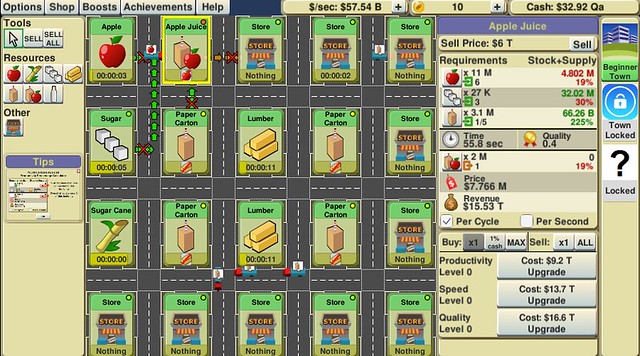
Look at that! Almost 33 quadrillion dollars. And we now have 66.25 billion paper cartons, enough for over 21000 batches of apple juice. With all that money, we have three major methods of increasing our income.
One is to improve the balancing by changing the mix of buildings; I can do that with six apple farms, three sugar mills (fed by six sugar cane farms), and one paper carton plant:

OK, that’s a factor of around five: \$57.54B/s → \$278.4B/s. We’re now at over 100% of all the required inputs for the apple juice factory. (A little notification popped up that I couldn’t screen-capture in time, saying ACHIEVEMENT COMPLETED Have Apple Juice production effectiveness at 100% +1 Idle Coins.)
The second method is to upgrade various plants, trying to achieve just over 100% on all the apple juice factory inputs — more than that, and there’s no benefit.

That pushed up my income by a factor of four. (\$278.4B/s → \$1.329T/s)
The third method is to upgrade to the next resource. I could try to make some more capital expenditures and upgrade using the cash I have… but I already have enough money to buy a milk factory (\$1.2 quadrillion dollars) and it earns 25× as much, so why bother with the apple juice factory anymore. The upgrade-to-the-next resouce strategy is almost always the best one, once you have enough money to do so.

Milk factories have no required inputs; perhaps the cows are hidden inside, along with some fields of grass. Once I can sell milk, the next production target is butter, and my goal is to build up enough cash to buy a butter factory.
The game goes on; there are some other quirks, like reaching the second town, or traffic slowdown if you have too many truck routes crossing town — but those are all the main aspects of gameplay. If you can upgrade your factories to manufacture chocolate cake, you’ve gone far and have reached a major accomplishment.
On the topic of upgrading: The breakeven graph I showed earlier is part of a subtle issue — I’ll call it the evolution-revolution dilemma — that you may encounter in Supply Chain Idle. I don’t think it has an exact parallel in the real world. Since it’s hard to capture game history statistics from Supply Chain Idle, I’ll make up a simplified equivalent example.
Suppose you have no starting money, but someone gives you a factory that produces income of \$1000 per second. (Fantastic, because that will put you at billionaire status in less than two weeks! Go retire!)
Now, you have three options for upgrading the factory at any given moment:
- Don’t upgrade at all, just let the money flow in.
- Evolution — upgrade your factory a little bit. For some amount of money, you can make an incremental improvement that will increase the factory’s rate of income by some modest factor K1. You can repeat this upgrade many times, but it will get more expensive each time by a factor K2 which is more than K1. (In Supply Chain Idle, this is like the productivity/speed/quality upgrades.)
- Revolution — if you manage to save up enough money, you can spend it on a major technology improvement that will increase the factory’s income a lot — say, by a factor of 100. It also costs a lot more than the evolutionary upgrade. (In Supply Chain Idle, this is like moving to the next output product, from apples to sugar cane to sugar and so on.)
The dilemma is what to do for an optimal strategy. It’s not at all obvious, and it depends on the numbers, but one way of describing this strategy is to perform some number (“i”) of evolutionary upgrades as soon as you have the cash on hand to do so (this is an example of a “greedy algorithm”), and then after that, save up until you can afford the revolutionary upgrade.
Let’s say the first evolutionary upgrade costs \$100K, so that takes 100 seconds to save up enough money. If K1 = 1.3 and K2 = 1.5, the options look like this:

The blue solid sawtoothy curve represents the amount of cash you have on hand if you keep performing evolutionary upgrades as soon as you can afford each one. If the revolutionary upgrade costs \$20M, the fastest way to get there is to stop after \( i=10 \) upgrades, which takes about 35 minutes — this brings your factory to an income of 1.310 × 1000 ≈ \$13786/second — and then wait until you build up the \$20M, which takes another 24 minutes, or about 59 minutes total.
If you keep doing evolutionary upgrades, it will take you a little longer to get to \$20M, about 79 minutes.
If you don’t do any evolutionary upgrades and let your factory build up \$1000/second, it will take you 20000 seconds to save up the 20 million dollars — that’s about five-and-a-half hours.
This effect is more pronounced with smaller evolutionary upgrades; here’s K1 = 1.03 and K2 = 1.05:
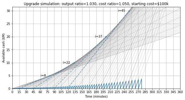
It would still take five-and-a-half hours to save up 20 million dollars with no upgrades, but it would actually take you longer than that if you keep using your available funds for evolutionary upgrades.
The fastest way to get \$20M with these parameters is to upgrade 37 times, which takes about 90 minutes, until you increase your income by a factor of about 3, then wait just under two hours to build up the cash.
So the spend-on-quick-upgrades vs. save-for-the-big-upgrades decision is an important one in Supply Chain Idle. (In the real world, things are slightly different; companies can take out a loan to finance CapEx costs that will improve their income.)
Takeaways from Supply Chain Idle
There are a few takeaways from this game that are at least somewhat relevant to semiconductor production, most of which are related to what I would call static supply chain optimization. (I have no idea what this is called in real life, so please pardon my lack of expertise.) In other words, there is an equilibrium where in most cases the supply chain will work best if all parts of it are used near 100% utilization: the rate of inputs of each production step is just enough to let that step run at 100% capacity. This is actually unrealistic, and we’ll explain why this is the case due to the dynamics of supply chains in Part Five. But for now let’s just work towards this nirvana of balanced 100% utilization.
-
Balancing: unless all rates of input material and production are matched at 100%, something has to wait. If the inputs are supplied below 100% of the required rate, the production machinery has to wait until there are enough inputs. If the inputs are supplied above 100% of the required rate, the excess input will have to wait until the production machinery is ready for it.
-
Bottlenecks: if there is one place that slows the whole process down, that is the best place on which to focus improvements to increase the rate of production. If I have everything needed to keep apple juice factories at 100% utilization except for the number of apples, then I should increase the number of apples. If everything is being provided at the right rate but my apple juice factory is processing the materials too slowly, then I should upgrade the factories to increase the rate of production. There are a couple of correlaries here; let’s say that there’s a production factory F producing output O from inputs A, B, and C. (Example: Factory F produces O = apple juice cartons from inputs A = apples, B = sugar, C = paper cartons.) The bottleneck for output O is the input that has the lowest supply rate, unless all input materials are arriving faster than they can be processed, in which case the bottleneck is factory F. (If input rates are A = 19%, B = 30%, and C = 225% of factory F’s capacity to produce 2 million cartons per minute, then A is the bottleneck, and factory F will produce 19% of its capacity, or 380,000 cartons per minute.)
-
If an input is not the bottleneck for O, then increasing its rate of supply has no effect other than to make more of it pile up in the factory. (For example, if I double the supply of sugar to increase it from 30% to 60%, then F will still produce 380,000 cartons per minute.) All that matters is the bottleneck, until it is no longer the bottleneck.
-
Since there are no sequential steps in this game, Amdahl’s law has no effect: if A is the bottleneck for O, and increasing the rate of A by some factor K will still leave A as the bottleneck for O, then the production rate of output O will also increase by that same factor K. (Example: if apples = 19%, sugar = 60%, and paper cartons = 225%, and I double apples from 19% to 38%, then apples is still the bottleneck and the factory will also double its production to 38%, or 760,000 cartons per minute.)
-
When there isn’t a single bottleneck (multiple inputs support the same rate of output production), then to increase the output O by some factor K, all of the bottleneck factors have to be increased by the same rate K. (Example: if apples = 30%, sugar = 30%, and paper cartons = 225% of factory capacity, then to double factory output I need to double both the rate of apple and sugar supply. If apples = 100%, sugar = 100%, and paper cartons = 225% of factory capacity, then to double factory output I need to double the rate of apple and sugar supply as well as double the factory processing capacity.)
-
-
Upgrade, upgrade, upgrade! There’s no competition in this game, but the only way to reach the more advanced production targets is to have enough cash to buy the latest factories, and the only way to earn that cash is to increase the productivity, speed, and quality of the factories and stores.
-
Technological advancements in the leading edge can make the trailing edge unprofitable. In Supply Chain Idle, as soon as you have enough money to buy a factory for the latest production target, and can start producing it, it’s no longer worth trying to make any of the earlier outputs, and all the old supply chains should be restructured to produce this new thing. The best use of capital expenditures is to make the most profitable output. (In the real world, it doesn’t exactly work this way.)
-
Pick the right balance of evolutionary vs. revolutionary upgrades. Don’t use up all the money to pay for the easier small productivity gains; make sure to plan for a larger gain (in Supply Chain Idle, the next production target) which can get to a better return, even if it means forgoing those small improvements.
Die Shrinks and Technology Nodes, Far From the Madding Crowd
Let’s go back to a fairly simple question that does not have a simple answer:
What is the best choice of technology node to design a chip?
There’s a more basic question to answer first: which technology node was used to design a chip? Very occasionally we do get some information from manufacturers. The leading edge tends to tout this quite a bit. Here’s Intel’s press announcement from 2009 on its Sandy Bridge 32nm architecture and 22nm technology:
INTEL DEVELOPER FORUM, San Francisco, Sept. 22, 2009 – Intel President and CEO Paul Otellini today displayed a silicon wafer containing the world’s first working chips built on 22nm process technology. The 22nm test circuits include both SRAM memory as well as logic circuits to be used in future Intel microprocessors.
“At Intel, Moore’s Law is alive and thriving,” said Otellini. “We’ve begun production of the world’s first 32nm microprocessor, which is also the first high-performance processor to integrate graphics with the CPU. At the same time, we’re already moving ahead with development of our 22nm manufacturing technology and have built working chips that will pave the way for production of still more powerful and more capable processors.”
The 22nm wafer displayed by Otellini is made up of individual die containing 364 million bits of SRAM memory and has more than 2.9 billion transistors packed into an area the size of a fingernail. The chips contain the smallest SRAM cell used in working circuits ever reported at .092 square microns. The devices rely on a third-generation high-k metal gate transistor technology for improved performance and lower leakage power.
Or Apple’s June 6, 2022 announcement of its M2 processor on 5nm technology:
CUPERTINO, CALIFORNIA Apple today announced M2, beginning the next generation of Apple silicon designed specifically for the Mac. Built using second-generation 5-nanometer technology, M2 takes the industry-leading performance per watt of M1 even further with an 18 percent faster CPU, a 35 percent more powerful GPU, and a 40 percent faster Neural Engine.1 It also delivers 50 percent more memory bandwidth compared to M1, and up to 24GB of fast unified memory. M2 brings all of this — plus new custom technologies and greater efficiency — to the completely redesigned MacBook Air and updated 13-inch MacBook Pro.
On the trailing edge: we don’t hear it as much. Microchip’s datasheet for the PIC16C54 — introduced sometime in 1989, according to a 1990 EDN issue on microprocessors — lists several revisions of parts in this series, along with the process technology used:

Antoine Bercovici (@Siliconinsid) graciously posted a composite of die shots of the PIC16C54, PIC16C54A, and PIC16C54C for me:
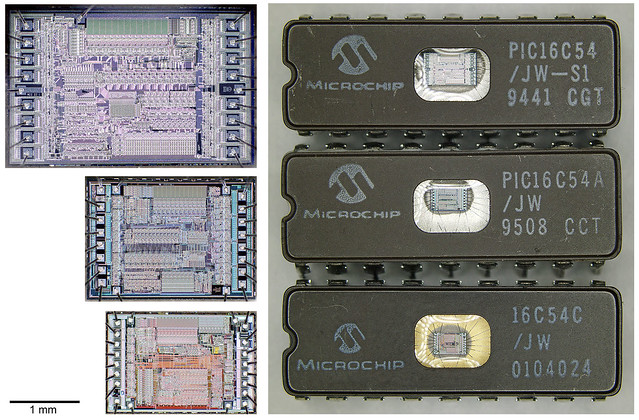
The “A” and “C” versions used smaller technology nodes, but if you look carefully you can see differences in the chip layout: this wasn’t just a photographic die shrink (again, see Ken Shirriff’s excellent article on the subject) and involved some significant layout changes.
Aside from the case of the PIC16C54, I’ve noticed that Microchip rarely states the feature size in its datasheets. For customers, why would it matter? It doesn’t change the functionality.
I got curious if this was the case in general — my experience has been that it’s rare to see the technology nodes listed in the datasheet or product brief. So I poked around a bit on the Internet, and here is my quick unscientific survey, including a smattering of ICs, mostly microcontrollers. I found information on node size more than I expected:
- Ambiq Apollo4 Blue (AMA4B) — not listed; reverse-engineering firm TechInsights claims it uses TSMC 22nm eMRAM
- Analog Devices Blackfin ADSP-BF70x — 40nm
- Espressif ESP32 — 40nm
- FTDI FT2232H USB ↔ UART converter — not listed
- Infineon SLC36PDx/SLC37PDx — 40nm
- Infineon PSoC 5LP — not listed in product page or product brochure or datasheet
- Infineon PSoC 6 — 40nm in product brochure but not in datasheet
- Microchip dsPIC33CK256MP508 — not listed
- Microchip dsPIC33EP256MC506 — not listed
- Microchip PIC12F508 — not listed
- Microchip PIC18Fx6Q71 — not listed
- Microchip SAM E70 series 32-bit ARM Cortex M7 — not listed
- Microsemi (Microchip) PolarFire FPGA — 28nm
- Nordic Semiconductor nRF9160 — not listed
- NXP S32G2 — 16nm
- NXP S32K1 — not listed in datasheet; 2016 marketing presentation mentions 90nm
- Renesas RL78 — 130nm
- Renesas RX600/RX700 — 90nm and 40nm
- Renesas RH850/C1x — 40nm
- Silicon Labs EFR32MG21 — not listed in datasheet, but EFR32 Series 2 press release mentions 40nm
- ST STM32U5 — 40nm
- ST STM32g0x0 — not listed
- Texas Instruments TMS320LF28335 — although the datasheet doesn’t list the node size, one of TI’s appnotes (SPRA9851) includes this footnote:
These estimates apply only to the devices covered by this report (see Section 1), which have all been fabricated in the same 180 nm CMOS process. The newest F28xxx devices (e.g. F28M35x, F28M36x) are fabricated in a 65 nm process and also have a wider flash pre-fetch buffer. They have significantly higher effective flash execution performance than the 180 nm devices.
- Texas Instruments TMS320C6455 — 90nm
- Texas Instruments MSP430x5xx, MSP430x6xx — not listed
- Texas Instruments MSP430FR58xx — https://www.ti.com/lit/wp/slay019a/slay019a.pdf) — not listed in the datasheet, but the FR58xx series was originally codenamed “Wolverine” in press releases which mentioned 130nm technology.
Analog chips (op amps, comparators, etc.) will rarely if ever list the feature size.
It’s hit or miss whether and how each manufacturer includes this information. My guess is they put it up as a marketing blurb if it suits them; otherwise they don’t. I seem to remember some engineer telling me a story that all the automotive companies need to know is the particular process used at a foundry (TSMC 180nm or 22ULP or whatever) and the die size, and they will tell the chip manufacturer, “OK, we’ll pay such-and-such a price” instead of letting the manufacturer tell them, because with this information they know roughly the cost of the die, and can figure out what profit the IC manufacturer ought to make, in their minds.
To get the die size and feature size — in theory — all you have to do is buy any chip, crack it open, and look at the die under a microscope, making appropriate measurements. There are, apparently, giveaways that make it possible to distinguish which company’s fabs it came from, at least if you know what to look for. (I don’t.) Reverse-engineering firms will do this, for a price. If you just want a photograph, to try to make measurements yourself, there are die shot enthusiasts like @Siliconinsid who will — if they are interested — decap and photograph IC die, as a hobby, especially if someone donates the ICs, and asks nicely.
One recently-produced microcontroller makes an interesting case study: the Raspberry Pi RP2040.

Raspberry Pi RP2040 die shot, top metal layer visible, © John McMaster, reproduced with permission.

Raspberry Pi RP2040 die shot, topmost metal layers removed, © John McMaster, reproduced with permission.
RP2040 Design Trade-offs
The RP2040 is an interesting case for several reasons, one of which is that the chip designers were interviewed on the electronics podcast, The Amp Hour, in February 2021.[21] (Raspberry Pi’s ICs and hardware are designed by Raspberry Pi Trading Ltd., a subsidiary of the non-profit Raspberry Pi Foundation, which is perhaps why the chip designers were given the freedom to talk a bit about their work; you are unlikely to hear this kind of detail from chip designers who work for the leading MCU manufacturers.)
According to the RP2040 web page, the microcontroller “builds Raspberry Pi’s commitment to inexpensive, efficient computing into a small and powerful 7 mm × 7 mm package, with just two square millimetres of 40 nm silicon.”
John McMaster took some high-resolution photographs of the RP2040 die, measuring it at 1.71 x 1.75 mm = 2.99 mm²; this discrepancy with Raspberry Pi’s “two square millimeters” may be a measurement of the die inside the I/O pads, which appears to be about 60% of the total die area.[22] Each pixel in these photographs is approximately 0.36 microns, making the I/O pads approximately 66 × 54 microns.
Why 40-nanometer technology? The Amp Hour podcast had this insightful exchange at 33:10, covering the decision to leave flash memory off of the RP2040, which requires circuit designers using the RP2040 to add nonvolatile memory externally:
Chris Gammell, host: So… could you give us a rough estimate, for like… the… I feel this is maybe touchy ’cause it’s asking about cost numbers, but like… obviously it was a cost driven decision, but like, was it enough of a… that seems like this is a decision that was made, like, right at the beginning. So like, how did this decision making process go to put flash external?
Luke Wren, hardware engineer: It, it’s definitely been one of our, our main design briefs, to make it as low cost as possible, and also to offer as much memory as possible, at the lowest possible cost. So we are roughly a 2 square millimeter device on 40 nm. We get about 20,000 die per wafer.
Gammell: Oh, wow!
Wren: It, it’s crazy, yeah. We actually, so this is the second, uh, iteration of this device; the, the first one was more of a test bed for the analog hardware. Um, this is B0, that was A0. On A0 we did actually have the flash on-die. We completely bottomed out on that development possibility. And we think that economically it’s the right thing to do.
So, that device had, uh, 256K of onboard flash, and 32K of onboard SRAM. And because flash is more dense than SRAM, that was a, a smaller device to, to produce. But actually, because of the, the extra passing [“pasting”? “passivation”?] steps in building the flash, it was the same cost as B0, which is a larger device. So, I think if you asked your average software engineer, would you like to trade all of your flash for SRAM at constant cost, and then spend a few cents if you need to initialize it or execute from an external device, they’d probably say yes, because bumping up against limited memory is one of the, the constant frustrations in, in embedded software, and, and actually SRAM can be as cheap as, as flash if you make some hard-nosed decisions on what else you have on die.
Gammell: Hmm. Well that’s a really interesting insight into that, into that uh … decision-making. I— I was just looking— I— when I first heard of— when I heard about this, I was just thinking like, flash is gonna be on an advanced node anyways, I mean it chases the leading, bleeding edge anyways, just so that flash makers can, can keep up, it feels like, I mean, having worked for one of them…
Wren: Yeah, but there are already people who are making silicon that’s really highly optimized to make flash at a low cost, and the 40nm process we’ve used with the metal stack we’ve used is great at making logic and SRAM at low cost. And actually, if you try and put those both on the same die, you might expect that integrating them makes it cheaper. It actually makes it more expensive.
James Adams, COO and hardware lead: I was gonna say, the net, the net cost is… probably slightly in favor of the external flash. Um… as Luke says… this kind of… you know, the… this stuff isn’t completely obvious, right? I think it was about 35% cost up to, to add flash to 40nm, something like that — don’t quote me on it exactly, but, you know, significant. And then you’ve added the flash on your die, and then you’ve taken away all of the space you can, where you can put your SRAM, right? And it’s a slightly more funky process than a standard 40 process that everyone knows and loves and all the IP is developed for, so you kind of… [chuckles] You also have to sign a bit of a waiver in your IP saying hey, we’re using this slightly funky flash process… uh… maybe your IP isn’t gonna work. So we kind of… after looking at the… after having the first initial, uh, test silicon, and looking at the whole thing in the round, it just made a lot of sense to put the flash external. And then also… of course then it gives you the flexibility to have as much or as little as you want, so that worked out very nicely.
There are some subtleties here — and I apologize if I get some of this wrong; I’m not a chip designer so my knowledge of these IC design tradeoffs is second-hand.
IP reuse
James Adams mentions the term “IP” in this interview. IP is “intellectual property”, understood in the semiconductor industry to mean a third-party design of a portion of a chip that can be reused. Chip design has changed over quite a bit over the years since the design of the 6502 (see Part Two), roughly paralleling the changes in software engineering since 1975:
-
Gradual shift towards high-level design with computer-aided tools — Digital designers today typically work in Verilog or VHDL, which are hardware description languages (HDL) to express the “source code” of a register-transfer level (RTL) design. EDA tools then synthesize the RTL down to an abstract network of logic gates, which the tools can then place and route on a particular IC, given the design rules of the fab process. Just as compilers have allowed programmers to work at a higher abstraction level, relieving them of the need to work in assembly language and to manage computation at level of the CPU registers and instruction set, RTL design uses digital abstractions to relieve the digital designers of the need to think at the kind of gate and transistor and layout level used in the 1970s. EDA tools are unlikely to squeeze out every last unnecessary transistor from a design, but they are faster than a manual effort, guarantee correctness, and are flexible to changes.
-
Reuse of third-party IP — The complete design of a microcontroller purely from scratch is no longer cost-effective. IP blocks for the CPU core or common peripherals (UART, SPI, I²C, etc.) are frequently purchased instead of designed and verified in-house. This makes it possible for a small team to design chips like the RP2040,[23] as system integrators, using HDL to connect the various blocks and to add whatever specialized logic is necessary.
IP companies are varied in size. Some are small and you’ve probably never heard of them; the largest is probably Arm Limited, which licenses the ARM CPU core. The first company to license IP for a CPU core was the Western Design Center (WDC) — founded by 6502 designer Bill Mensch in 1978 — which began licensing the 65C02, an improved CMOS adaptation of the MOS 6502, in 1981.[24]
WDC still licenses the W65C02 today in several forms, including educational licenses for engineers to learn about chip design using CPUs such as the W65C02 and W65C816. The different forms include “hard”, “firm”, and “soft” IP, according to WDC’s website:
- “soft” IP is an RTL design in Verilog
- “firm” IP has been synthesized to a network of gates for use on an FPGA
- “hard” IP has been optimized manually into physical transistor designs, implemented in GDSII form, for various feature sizes from 3 µm down to 350nm. (Mensch states: “We plan to scale the W65C02S and W65C816S to 180nm implementation with universities that want their students to create projects with the manually optimized chips. There is an educational opportunity in learning how manual design, scaling and resizing was used historically for various processes.”[25] In smaller feature sizes, the cost of the silicon is so low that the advantages of manual optimization are not economically useful, and, as Mensch points out, “don’t have the manufacturing flexibility of HDL languages.”)
The RTL form, because it’s an abstract digital design, can be implemented on any modern fab process. It makes me curious to think of how small the W65C02 would be on 3nm, and how fast it would operate....
Analog and mixed-signal IP, because it doesn’t permit the same kind of abstraction as digital design, is generally provided as “hard” IP aimed at a specific fab process.
Die area requirements
Several other significant issues in the RP2040 design involve the constraints and die area requirements of memory.
Flash memory and DRAM and ROM each have so-called “1T” designs, meaning that a single transistor can be used to hold one bit of data. (Modern stand-alone NAND flash uses multilevel cells which allows a single transistor to hold several bits of data.) SRAM, on the other hand, is conventionally a “6T” design — six transistors are required for each bit: four for a pair of inverters forming a flip-flop, one to read the contents onto an output line, and one to write the contents from an input line. So SRAM costs around six times as much area as an equivalent amount of flash memory or DRAM or ROM, if the memory cell transistors are minimum size for the lithography process. This is why you’ll generally see microcontrollers with around a 4:1 / 8:1 / 16:1 ratio of program memory to data memory: a 4:1 ratio should mean that the SRAM area is around 1.5× as large as the program memory, so it’s heavy on the SRAM. An 8:1 ratio means the SRAM area would have about 75% of the area as program memory, and 16:1 ratio means that the SRAM area has around 37.5% of the area as program memory, so it’s heavy on the program memory. It would make no sense to design a chip with an extreme ratio of program to data memory like 128:1, for example, and spend silicon area of, say, 1 megabyte of flash memory and only 8 kilobytes of SRAM — in this case the SRAM would take up only around 6/128 = 4.7% of the area of the flash — when putting twice as much SRAM would increase the cost by only a little bit to get a 64:1 ratio.
Flash memory puts extra constraints on the fabrication process, which is why you’re not seeing tons of microcontrollers coming out on 7nm or 5nm silicon; advanced nonvolatile memory is now around the 16nm / 22nm / 28nm range.[26][27][28] Some of the mainstream MCU manufacturers — Renesas,[29] ST,[30] and Infineon[31] — have parts in production using proprietary 28nm processes with embedded flash. The RP2040 designers chose to give up using on-chip flash memory to save cost, using SRAM instead — even though SRAM would be larger than an equivalent amount of flash.
SRAM has one big advantage over flash memory, which is that the read time is faster, and in some microcontrollers — like TI’s TMS320F28335 DSP and others in its C2800/F2800 series — the CPU is fast enough that the use of flash for program memory requires several clock cycles (“wait states”) to access an arbitrary given memory location. So executing out of SRAM is faster, if you don’t mind using up some of your RAM to hold critically-fast sections of program memory. Modern processors use memory caches to speed this up, and the RP2040 has one, the so-called “XIP” (eXecute in-place) cache to speed up execution from off-chip flash. (The next instruction’s in the cache? Great, no wait. Not in the cache? Time to wait....)
Let’s look at that die photograph again, but this time with some annotated sections I have added.[32][33][34]

Base image: Raspberry Pi RP2040 die shot, top metal layer visible, © John McMaster, reproduced with permission.
The outer sections of the chip are dedicated to I/O pads and drivers; the remaining inner areas of the chip are annotated above and have the approximate areas shown below. (These are based on my pixel measurements of the image, relative to John McMaster’s 1.71 × 1.75 mm die measurements; the exact values of the numbers are not as important as just trying to get a general point across.)
name memory area (mm²) % SRAM banks 0-3 256 kB 0.672 22.5% random logic 0.589 19.7% VREG 0.153 5.1% USB PHY 0.089 3.0% ADC 0.080 2.7% XIP cache 16 kB 0.066 2.2% clock gen 0.039 1.3% USB DPRAM 4 kB 0.031 1.0% SRAM banks 4-5 8 kB 0.030 1.0% ROM 16 kB 0.017 0.6% The brown areas are memory. The gray areas are analog, power, or other functions that require specialized transistor sizes and layouts. The purple area annotated “random logic” (also known as “sea-of-gates”) consists of the transistors that the IC design software placed to implement general digital features, and would include all the digital peripherals and the CPUs.
The SRAM banks 0-3 are large enough that we can benchmark the effective SRAM cell size: 256 kB = 2097152 bits in 0.672 mm² → 0.32 µm²/bit.
At 40nm, this is consistent with a graph of commercial SRAM cell sizes I found in a VLSI lecture:[35]
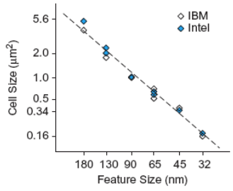
TSMC itself claims, on its 40nm page:
TSMC became the first foundry to mass produce a variety of products for multiple customers using its 40nm process technology in 2008. The 40nm process integrates 193nm immersion lithography technology and ultra-low-k connection material to increase chip performance, while simultaneously lowering power consumption. This process also set industry records for the smallest SRAM (0.242µm² ) and macro size.
I don’t know whether this is for raw SRAM cell size, or whether it includes the overhead of the read/write circuitry; the “hot cross bun” appearance of the SRAM is, according to a UC Berkeley lecture note,[36] because large arrays are “constructed by tiling multiple leaf arrays, sharing decoders and I/O circuitry.”
Notes
[21] Chris Gammell, Podcast 529: Embedded Hardware with the Raspberry Pi Team, The Amp Hour Electronics Podcast, Feb 7 2021.
[22] Using John McMaster’s web viewer, I measured the die dimensions in pixels as 4860 × 4720, with the inner rectangle (excluding I/O pads) at approximately 540 pixel margin from each edge; (3780 × 3640)/(4860 × 4720) ≈ 0.5998.
[23] In Chris Gammell’s Amp Hour podcast, the RP2040 team was “small”, according to Adams. in a September 2017 interview, Raspberry Pi Trading’s CEO mentioned there were around 25 engineers in the entire company, including software and hardware engineers, many of whom were involved in working on the various iterations of Raspberry Pi and other development boards. Development of the RP2040 was started about that time, in summer 2017, according to Liam Fraser, so it’s possible that the three engineers Gammell interviewed made up most of the chip design team.
[24] Mensch had left MOS Technology in March 1977, about six months after MOS was acquired by Commodore. For the next year or so, he had been working at Integrated Circuit Engineering as a consultant, training engineers at various companies how to design microprocessors, when Chuck Peddle called him, saying that Jack Tramiel, Commodore’s founder and CEO, wanted Mensch to design calculator chips at Commodore. Mensch had been wanting to get back to chip design, and within ICE would not have been able to do so; among other reasons, there was bad blood between Tramiel and ICE’s chairman Glen Madland. So Mensch struck out on his own, and in May 1978 met Peddle and Tramiel — at a Las Vegas casino, where Tramiel enjoyed high-stakes gambling — to negotiate an agreement to help start Mensch’s company.
At WDC, Mensch worked exclusively with Commodore for over two years on the design of calculator ICs, until Tramiel pulled out in October 1980, amid Commodore’s business failure in the calculator market. According to Mensch, “WDC delivered both a five function (LC5K3) and a scientific (4500 4-64-bit RISC) calculator chips intended under WDC-CBM contract.” (Peddle departed Commodore in September 1980, after a disagreement with Tramiel.)
In 1981 Mensch began designing the CMOS 65C02, and licensed it to GTE for use in telephone systems. (Fortunately for Mensch, Commodore had never expressed interest in a CMOS version of the 6502, at least not through Tramiel and Peddle. Mensch adds, “That said, after Tramiel was fired from CBM during a CES show, a representative of CBM came to Phoenix to settle an ongoing lawsuit between CBM and WDC. Part of the lawsuit settlement was that CBM would pay WDC to license the W65C02 and W65C22 at ½ WDC’s traditional license fees. Interestingly WDC would not license CBM with the same deal on the W65C816. The CBM representative said they were planning to use the Intel x86, which they never did, and had no interest in the 65816 at that time. The C128, selling 5 million units, used a weird combination of the 6502 and Z80.”) GTE manufactured the 65C02, apparently selling it to external customers as well as for its own equipment: in spring 1982, Apple received the first 65C02 chips destined for what became the Apple IIc. Mensch got into the fabless semiconductor IP business in 1984, almost by accident: Apple was working on the IIgs at the time, designed around WDC’s 65816 processor, and had lined up GTE and NCR as two sources for manufacturing it, when NCR pulled out at the last moment and Mensch, thinking quickly, offered to second-source the chips himself by having them fabricated by any manufacturer satisfactory to Apple. Mensch negotiated with Sanyo to manufacture the 65816.
Sources:
-
Stephen Diamond (interviewer), Oral History of William David “Bill” Mensch, Jr., Computer History Museum, Nov 10, 2014. My summary of how Mensch got into designing the 65C02 doesn’t do the story justice; read the CHM interview.
-
Bill Mensch, personal communication, Nov 24 2022 and Dec 4 2022, including the direct quotes.
-
Brian Bagnall, Commodore: A Company on the Edge, 2010.
-
Selby Bateman, Bill Mensch — The Brains Behind the Brains, Compute!’s Apple Applications Special Issue, Fall/Winter 1986.
-
Western Design Center Inc., “About Us”, website.
[25] Bill Mensch, personal communication, Dec 4 2022.
[26] Mark LaPedus, Embedded Flash Scaling Limits, Semiconductor Engineering, Jul 19 2018.
[27] Shannon Davis, Weebit Scaling Down its ReRAM Technology to 22nm, Semiconductor Digest, Mar 15 2022.
[28] Peter Clarke, TSMC offers 22nm RRAM, taking MRAM on to 16nm, eeNews Analog, Aug 25 2020.
[29] Peter Clarke, Renesas samples 28nm MCUs with embedded flash, eeNews Automotive, Mar 27 2018. The Renesas MONOS flash technology was apparently a collaboration with TSMC.
[30] Roger Forchhammer, Automotive MCUs in 28nm FD-SOI with ePCM NVM, ST Microelectronics, Sep 12 2019.
[31] Infineon, Embedded Flash IP Solutions. Infineon claims “Infineon’ SONOS eFlash has been in production since 2001 on 350 nm and 130 nm nodes, and is now available on 65 nm, 55 nm, 40 nm and 28 nm nodes.” — but it mentions details only for 55nm and 40nm, along with temperature grades up to Automotive Grade 2 (-40°C to +105°C) which leaves out the Grade 1 and Grade 0 applications. See also Cypress SONOS eFLASH.
[32] Raspberry Pi RP2040 home page. There’s a nice annotated version of John McMaster’s photograph, with sections of the die labeled in a stylized fashion — so I am making what I hope is a reasonable assumption that the labels are directly on top of the corresponding silicon.
[33] Luke Wren (one of the RP2040 designers), Twitter, Feb 2 2021: “From left to right this looks like cache data RAM, cache tag RAM, USB DPRAM”, commenting on a photo posted by John McMaster.
[34] Raspberry Pi RP2040 datasheet
[35] David Matthews, Lecture 19: SRAM, University of Iowa ECE 55:131 Introduction to VLSI, 2011.
[36] John Wawrzynek, Krste Asanović, John Lazzaro, Yunsup Lee, Lecture 8: Memory, University of California Berkeley, CS250 VLSI Systems Design, Fall 2010.
Myths and Reality
So there you have it: a quick look at some design issues around the Raspberry Pi RP2040. But that only hints at an answer to the question I asked at the beginning of this section:
What is the best choice of technology node to design a chip?
To get a better sense of an answer, we have to look at some industry myths, which all dance around this issue.
Myth #1: Oh, You Should Just Go To 28nm
(Amdahl’s Law, Die Shrinks, and HHG Cost Modeling)
There are some indications that the foundry industry will have lots of 28nm capacity in the future, much more than 40nm or 65nm or other mature nodes,[37] and the peanut gallery staring at this train-wreck-of-a-chip-shortage is shaking their heads, wondering why IC designers aren’t just using 28nm for new designs. (There does seem to be a general recognition that once you go away from planar transistors to FinFETs below 28nm, that things get more difficult and more expensive.)
The main driver pushing towards 28nm besides available capacity is Moore’s Law cost advantage. Here’s a slide from Intel’s 2017 Technology and Manufacturing Day:
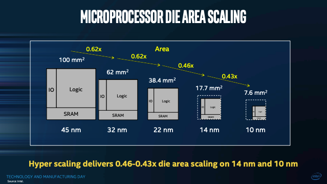
Source: Intel Corporation[38]
Look at that amazing decrease. A 45nm design that takes a 100 mm² die is projected to shrink down to a 7.6 mm² die at 10nm; Intel figured out a couple of extra tricks at 14nm and 10nm, which it calls “hyper scaling”, to increase transistor density.[38]
As far as the transistor density of TSMC’s 40nm vs. 28nm, their 28nm technology webpage used to contain a short statement:
TSMC’s 28nm technology delivers twice the gate density of the 40nm process and also features an SRAM cell size shrink of 50 percent.
The low power (LP) process is the first available 28nm technology. It is ideal for low standby power applications such as cellular baseband. The 28LP process boasts a 20 percent speed improved over the 40LP process at the same leakage/gate.
So we might expect, at first guess, that a 28nm RP2040 would be able to yield 40,000 die per wafer instead of the 20,000 die per wafer for the 40nm RP2040. More die per wafer = lower cost, right?
Well, not quite.
Using a smaller technology node may make sense in some situations, but there are some reasons why going to a smaller node does not make sense.
-
Cost goes up. Scotten Jones, one of the world experts on semiconductor cost modeling, published a great post called LithoVision – Economics in the 3D Era,[39] in which he pointed out that for modest production runs, the cost per wafer of smaller nodes skyrockets:
From the figure and table, we can see that mask set amortization has a small effect at 250nm (1.42x ratio) and a large effect at 7nm (18.05x ratio). Design cost amortization is even worse.
The bottom line is that design and mask set costs are so high at the leading edge that only high-volume products can absorb the resulting amortization.
So something like the RP2040 would need to have upwards of 2000 wafers to bring down the mask set cost at 28nm to a small fraction of the total manufacturing costs. (And at 20,000 die per wafer that’s a run of 40 million die; at 40,000 die per wafer that’s 80 million die!)
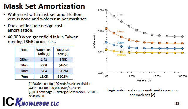
Slide used by permission of IC Knowledge LLC.
If the assumption here is that there is a fixed mask set cost \( M \) (shown in Jones’s data) and then a fixed cost per wafer \( w \) regardless of volume, then the wafer cost ratio shown in the table \( \rho = \frac{w + M/100}{w + M/100000} \) can be solved for \( w = M\frac{1000-\rho}{(\rho-1)\cdot 100000} \) along with breakeven volume \( V=M/w \):
feature size mask set cost \( M \) wafer cost \( w \) breakeven volume \( V \) 250nm \$43k \$1022 42 90nm \$165k \$1647 100 28nm \$1200k \$2955 406 7nm \$10500k \$6047 1736 Feature size comes down, cost goes up. The whole point, though, is that at smaller feature sizes the cost per transistor at high volumes comes down, which is a big reason why all the latest advanced chips keep wanting to push towards 5nm, 3nm, 2nm, etc.
Jones published an interesting set of slides on “Technology and Cost Trends at Advanced Nodes”[40] showing relative wafer costs and density for various TSMC processes, presumably showing the costs at high volumes:
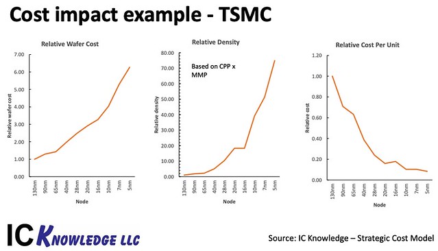
Slide used by permission of IC Knowledge LLC.
The effective cost per unit appears to be a decrease of a factor of around 1.6 (= a multiplier of 0.625) from 40nm to 28nm. (This results from a 2× density increase, but a cost per wafer increase of 25%.) This is 2016 data, but Jones’s LithoVision 2020 presentation also mentions that Intel and all the major foundries had an average cost per transistor trend of 0.6× per node from 130nm to 28nm.
If I’m an IC designer working on a high-volume project, and I want to use the next node, this is just great:
- I can pay 20% more for 2× as many transistors in the same area
- I can pay about the same as the last chip to get 1.66× as many transistors in 83.3% of the area
- I can pay 40% less for the same number of transistors in half the area (this has its own issues though; stay tuned)
But if my volumes aren’t that large, I lose: the increase in one-time setup costs at 28nm outweighs any financial savings of lower cost-per-transistors. (We’ll take a more detailed look at this in just a moment.)
-
Increased complexity and constraints. There are a number of reasons that not only are designs at advanced nodes more difficult, but that they may be limited to a minimum feature size that is larger than the leading edge. Some designs (like the RP2040, which isn’t an automotive IC and isn’t using onboard flash memory) aren’t subject to all of the following issues, but that doesn’t mean there will be a painless migration from 40nm to 28nm:
-
IP availability — in addition to nonvolatile (Flash) memory, which I have discussed already, some of the IP like the ADC may not be available at 28nm, or may raise cost significantly.
-
Voltage tolerance — Dennard scaling says that my supply voltage has to come down in order to make Moore’s Law work. We’re way past the old days when 5V microprocessors and microcontrollers were common. Nowadays the CPU core voltages for processes in the “mature node” range used for microcontrollers (say, 28nm - 130nm) are in the 0.9 - 1.5V range.[41]
-
Temperature tolerance — automotive designs need a wider range of temperatures — -40°C to +150°C for AEC Q100 Grade 0[42] — than consumer applications, and there’s an expectation of longer operating lifetimes with lower failure rates.
Source: Monolithic Power Systems, Fundamentals of AEC-Q100: What “Automotive Qualified” Really Means.[43]
-
-
Not everything scales down with feature size. The memory and random logic should shrink by half; those are easy beneficiaries of Moore’s Law. But components of the chip that aren’t based on minimum transistor size don’t benefit. This includes the I/O pads, which have a minimum size for bond wire attachment, and for the drive circuitry. (Those drive transistors have to dissipate power somehow.) The components I highlighted in gray — USB physical layer, voltage regulator, clock generator, and ADC — are also unclear whether they benefit from scaling. I suspect that the voltage regulator scales down if the power consumption goes down. This is one benefit of moving the same number of transistors to a smaller feature size at the same clock rate… at least until we reach smaller feature sizes that have made subthreshold conduction a significant part of power dissipation.[44] The clock generator may also scale with overall chip area, since its job is to drive a whole bunch of gate capacitance. The USB PHY is a wild card; it has to drive external logic, and I would have guessed it couldn’t get much smaller due to those drive requirements, but here is the RP2040 sporting a 0.09 mm² USB PHY, whereas I found an article from 2006[45] claiming that common USB PHY IP took 1.0 - 1.2 mm² in the 180-130nm process range, with contemporary improvements in the 90-65nm bringing the area down by about half. The ADC and other analog sections are least likely to scale down with feature size: analog accuracy needs enough area to reduce error tolerance.
At any rate: Let’s be generous and say that everything but the ADC and I/O pads would scale down to half the area if the RP2040 went from 40nm to 28nm. That’s a fraction \( \alpha= \) 56.3% of the chip area.
Amdahl’s Law lets us calculate the increase in overall density in when a fraction \( \alpha \) of the chip area can be increased in density by a factor of \( N \):
$$s(\alpha,N) = \frac{1}{\frac{\alpha}{N} + (1-\alpha)}$$
If \( \alpha=0.563 \) and \( N=2 \) then we can calculate an overall density increase of 1.39: the new chip area should be about 0.72 as much as the old chip area, and we should be able to get 1.39× as many redesigned RP2040 chips out of a 28nm wafer — hypothetically, so that’s about 28,000 chips per wafer! — compared to the 40nm version. But the cost per wafer is expected to be 20% higher and I’ll have to sell 10 million of them if I want mask set costs to stay below 10% of my cost of goods.
In some cases, scaling digital logic down has no impact on the die size at all, because the I/O pads cannot be moved any closer together; these are pad-limited designs, as opposed to core-limited designs. As an example, here’s a layout image of the W65C02S, implemented on 0.6μm:

W65C02S image © Western Design Center, reproduced with permission
Here the core makes up about 35% of the total die area. Going to a smaller process would allow the core to get smaller, but because of I/O pad limitations would not reduce the die size.
The gist of all this is that it makes sense to use newer fab processes when the expected revenue is much higher than the one-time costs, and the cost of the scaleable transistors decreases. If sales volumes are small, or the cost per chip needs to be small, or the I/O pads and other power/analog circuitry that won’t scale down makes up a significant fraction of the chip area, then it’s not worth it to use the leading edge.
My guess is that even if every part of the RP2040 design were possible to move from 40nm to 28nm, and that 1.6x improvement of Moore’s Law were possible, the increase in one-time overhead costs at 28nm would be enough to warrant staying at 40nm. Here’s where cost modeling comes into play, and companies like Jones’s IC Knowledge earn their living. (And we as members of the general public only get a tiny glimpse, unfortunately.)
If that sounds too handwavy, we can do some of what I call “horseshoes and hand grenades” (HHG) cost modeling which is close enough to get a very rough quantitative understanding of the economics here. (If you’re going to spend the \$\$\$\$ to design a chip, you probably should do some more careful cost modeling, with validated assumptions, before you pick a node size.)
Here are my assumptions, based on Jones’s published slides and some of the Raspberry Pi RP2040 disclosed information:
- Mask set costs \( M \) can be interpolated on a log-log plot from the 250nm/90nm/28nm/7nm Lithovision 2020 data; I come up with a fit of \( M \approx 211000 f^{-1.557} \) where \( f \) is the feature size in nanometers and \( M \) is the mask cost in thousands of dollars
- Design cost \( D \) is either 5× or 10× the mask set cost \( M \) (that is: \( D = k_DM \) with \( k_D = \) 5 or 10) — this is less extreme than the IBS graph of rising design costs (see the section Not Fade Away), but my intuition is that these design costs are based on the assumption that the design complexity also goes up with each new node. This is probably my weakest assumption; if anyone has a suggestion on a better way to come up with an HHG-class estimate, I’d love to hear it.
- The die is small enough that yield losses can be neglected — or at least the yields are in the high 90% range and are similar for all the feature sizes listed below
- 28nm:
- \$1200K mask set cost
- \$2955 wafer cost
- costs 25% more for a wafer than 40nm (eyeballed from Jones’s graph in the Technology & Cost Trends presentation)
- permits twice the transistor density of 40nm, as per TSMC’s archived technology page
- 40nm:
- estimated mask set cost \( M \approx \) \$680k, from the interpolation formula
- wafer cost \( w \approx \) \$2360 (factor of 1.25 below 28nm, as stated above)
- a wafer yields 20,000 good die (RP2040 staff Amp Hour interview claimed 20,000 die, I’m neglecting yield losses as I stated earlier)
- 65nm:
- estimated mask set cost \( M \approx \) \$320k, from the interpolation formula
- wafer cost \( w \approx \) \$1840 (12% higher than 90nm wafer cost, eyeballed from Technology & Cost Trends graph using wafer cost ratios 1.3 for 90nm and 1.45 for 65nm)
- transistor density is a factor of 2.35 lower than 40nm, as per TSMC’s technology page on 40nm
- 90nm:
- \$165K mask set cost
- \$1647 wafer cost
- transistor density is a factor of 2.0 lower than 65nm, as per TSMC’s technology page on 65nm
- There are not significant decreases in price with volume so the total cost to make \( N \) wafers is \( C = M (1 + k_D) + Nw \) where \( w \) is the wafer cost. (The constant-price-per-wafer assumption is probably not true in the real world, but I don’t have any better information, and we could always break it down to a fixed initial cost that is lumped in with the mask set cost.)
- The fraction \( \alpha \) of the die area at 40nm that depends on the transistor density is either \( \alpha = 0.563 \) (as estimated above) or \( \alpha = 0.667 \) (being more optimistic); the rest of the die is constant area, mostly devoted to I/O pads and driver circuitry.
Again: I do not claim that these assumptions are correct; I’m just guessing that they’re somewhere in the right ballpark, so let’s see where they land.
I’m going to plot the unit die cost versus the number of die manufactured, using these assumptions:

Huh, that’s interesting. (The dot-and-lawnchair lines below each curve represent the asymptotes of per-unit cost and up-front cost, along with the breakpoint where they cross at the point where up-front cost per die equals unit cost per die. The lower graph is just a zoomed-in version of the upper graph.)
A few observations:
- Per-unit costs (from the marginal cost for each extra wafer) dominate at high volumes, and decrease with decreasing feature size
- Up-front costs (mask set and IC design) dominate at low volumes, and increase with decreasing feature size
- Cost for very high volumes at 28nm (10 or 11 cents per die) isn’t that much below 40nm (12 cents per die)
- The breakpoint between these regimes increases with decreasing feature size: the crossover in cost between 90nm and 65nm is on the order of 10M die, whereas the crossover in cost between 65nm and 40nm is on the order of 50M die, and the crossover in cost between 40nm and 28nm is on the order of 200M die.
Unless the Raspberry Pi folks expect to sell hundreds of millions of these things, they’ve probably made the right choice of 40nm. (And I’m going to assume that since they’ve shelled out the money to actually design and manufacture silicon, they’ve gone through much better analysis with much higher confidence that 40nm is right.)
We can plot the same kind of results for a larger die with mostly digital content; for a hypothetical “Microprocessor X” (“μP X”) I guessed at die size of around 80mm² on a 40nm process, yielding about 800 die per 300mm wafer, with 95% of that area comprising content that shrinks/grows with transistor density, and the other 5% taking a fixed area:

Here the same sort of general behavior applies (wafer costs dominate at high volumes, but mask set and design costs dominate at low volumes) but there are two differences:
- Cost savings at 28nm at high volumes are much larger than in our small-die RP2040 example, because more of the die size can be shrunk to take advantage of the higher transistor density.
- The breakpoint to reach the point where wafer costs dominate is much smaller than in the small-die case. We only need to sell 3M-5M units to justify the extra design costs of going to 28nm.
A good example of a chip in this category is the CPU in Apple’s iPhone series. Apple sells something like 200 million mobile phones a year.[46] Its CPUs have come out regularly, as predictably as hurricane season, once a year in September, since the A6 chip in 2012. The A6 was about a 97 mm² die produced using Samsung’s 32nm process.[47] In September 2021, the A15 chip was released, measuring in at about 108 mm²,[48], reportedly using TSMC’s 5nm process.[49] At these sorts of die sizes, and with volumes around 200 million, the leading-edge transistor density improvement justifies the high design and mask set cost — otherwise an earlier process would provide a lower cost, and Apple would just use that process instead.
(There are other reasons to use newer processes besides cost, namely the improvement in performance-vs.-power-consumption, but in the ultra-high-volume consumer market, it’s hard to beat cost as the primary driver. Apple’s A16 chip, using TSMC’s 4nm process, allegedly cost \$110 each, 2.4 times as much to manufacture as the A15[50] — but Apple must think it’s worth the increase in functionality and in value to its customers. Remember the fine print in Moore’s original 1965 article: The complexity for minimum component costs has increased at a rate of roughly a factor of two per year. That doesn’t mean transistor density increases at a near-constant rate per year, or that cost per transistor decreases at a near-constant rate per year — although both have kept up fairly well so far — but rather that the complexity in order to get the lowest cost per transistor increases, and maybe we’re reaching the point where gains in density and cost are running out, and the only way to make Moore’s Law gains is at the ultra-high end, letting the number of transistors in an IC skyrocket, even though it costs more and more.)
But for microcontrollers, needing fewer transistors and a lower-cost, smaller die, where significant portions of the die area do not shrink on a smaller process, the economics of the leading edge does not make sense.
Myth #2: The Node Name Actually Corresponds to Transistor Size
The industry has been talking about 5nm, 3nm, 2nm nodes lately. The transistors aren’t actually that small, though.
A recent article in IEEE Spectrum put it this way:[51]
But after decades of intense effort and hundreds of billions of dollars in investment, look how far we’ve come! If you’re fortunate enough to be reading this article on a high-end smartphone, the processor inside it was made using technology at what’s called the 7-nanometer node. That means that there are about 100 million transistors within a square millimeter of silicon. Processors fabricated at the 5-nm node are in production now, and industry leaders expect to be working on what might be called the 1-nm node inside of a decade.
And then what?
After all, 1 nm is scarcely the width of five silicon atoms. So you’d be excused for thinking that soon there will be no more Moore’s Law, that there will be no further jumps in processing power from semiconductor manufacturing advances, and that solid-state device engineering is a dead-end career path.
You’d be wrong, though. The picture the semiconductor technology node system paints is false. Most of the critical features of a 7-nm transistor are actually considerably larger than 7 nm, and that disconnect between nomenclature and physical reality has been the case for about two decades. That’s no secret, of course, but it does have some really unfortunate consequences.
The feature size originally referred to the metal half-pitch and minimum MOSFET gate length. From a 2014 article in Semiconductor Engineering:[52]
If we go back to the early 1990s, all was well in semiconductor technology nodeland. The metal half-pitch and the “gate length” were all in agreement, and a 0.5µm or 0.35µm process meant that those dimensions all lined up. Typically, the microprocessor process development teams were pushing for faster clocks to get more performance and so were trying to aggressively shrink gate lengths while memory (DRAM) process development teams were trying to reduce half-pitch in order to cram more bits onto a chip. This in part led to a divergence.
Nowadays the critical dimensions are generally contacted gate pitch (aka CPP = “contacted polysilicon pitch” even though polysilicon gates haven’t been used since the 45nm node) and minimum metal pitch (MMP) — the product of CPP and MMP is widely used as a marketing figure of merit for process density.[53][54] These are more important now than gate length in determining how small a standard “cell” can be made. From a 2018 EETimes article about the leading edge FinFET processes, showing an example of such a cell, with two transistors forming what appears to be an inverter:[53]
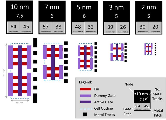
© Synopsys, Inc., reproduced with permission.
The dimensions for 5nm and smaller nodes were projected based on information available in 2018 when the EEtimes article was published.CPP represents the width of the cell. The height of the cell is proportional to the MMP.
IEEE Spectrum had an article in 2009[55] listing node names, metal half-pitch, and gate lengths, according to data from the International Technology Roadmap for Semiconductors (ITRS): (dimensions in nanometers, gate length = effective gate length)
Node Half-pitch Gate length 500 500 500 350 350 350 250 250 200 180 230 140 130 150 65 100 100 45 90 90 37 65 90 32 45 68 38 32 52 29 So the names of technology nodes are “feature sizes” that are veering away from physical reality.
Intel describes many of their fab processes in IEEE papers[56] with geometric data aside from transistor density, but in 2017 held a presentation covering transistor density[57]. TSMC does not seem to be as open about this kind of data for their processes, but Scotten Jones at IC Knowledge LLC has been tracking many of the leading-edge fab presentations at technical conferences, and has published some comparative data for various leading-edge processes in a recent article.[58] I’ve graphed data from both these sources pertaining to Intel and TSMC:

I’ve mentioned MMP, CPP, and gate length already; the lengths \( \lambda_{SRAM} \) and \( \lambda_{D} \) are characteristic lengths based on the square root of SRAM cell area and the reciprocal square root of transistor density.
The transistor density and SRAM cell data doesn’t seem quite consistent; the product of 6T SRAM bit area and transistor density should be about 6, which should show up in my graph below as a difference of \( \sqrt{6} \approx 2.45 \), but it’s not, until recent nodes. Perhaps SRAM had been heavily optimized at earlier nodes, compared to general transistor transistors? Who knows.
Also, nobody seems to care anymore about gate lengths since EUV has come into the picture.
The point is that feature size is just a generic number that’s sort of vaguely indicative of transistor density, but even that has veered away from a realistic measurement in recent leading-edge processes — look at the \( 10f \) line in the graph and how the SRAM and transistor density points are starting to go above that line.
Myth #3: 200mm wafer fabs are being displaced by the more economical 300mm wafer fabs
In Part Two, I mentioned that the MOS 6502 was originally produced using 3-inch silicon wafers. The wafer size has been creeping up over the years — 3-inch is essentially 75mm, and then came 100mm, 125mm, 150mm, 200mm, and 300mm — to drive down the per-unit cost even though the capital equipment cost has been rising.
Integrated Circuit Engineering (ICE) wrote a whole chapter on this trend — Changing Wafer Size and the Move to 300mm.[59] At the time this report was written, in 1997, 150mm wafer fabrication was plateauing and 200mm fabrication was zooming upwards, as you can see in Figure 7-1:

Hey, that looks just like the DRAM life cycle graph from Part Two:
© Randy Isaac, reproduced with permission.
But there’s a difference. DRAM has been continuing the trend — we’re up to 16 gigabit today — whereas wafer size improvements have stalled. Here’s more or less where we are today in 2022:
- 450mm fabs: never arrived in mass production
- 300mm fabs: mainstream for all recent silicon processes
- 200mm fabs: still around, primarily for mature nodes; also state-of-the-art for MEMS devices and other semiconductor materials such as silicon carbide (SiC) and gallium nitride (GaN), both of which are wide-bandgap materials experiencing rapid growth for power electronics applications
- 150mm fabs: mainly for MEMS, SiC, GaN, etc.; decreasing in importance (IC Insights published wafer capacity data for ≤150mm fabs is about 6% of total worldwide production[60])
The 200mm - 300mm gap is kind of interesting. For mainstream silicon processes, 200mm is essentially synonymous with anything 130nm and above (legacy nodes), with 300mm essentially synonymous with 90nm and below — namely processes that were introduced after 300mm equipment became available. This split between 130nm and 90nm does have some exceptions: for example, TSMC’s 300mm “GIGAFAB” facilities cover 130nm, 90nm, 65nm, and below; UMC’s fabs, which I mentioned earlier from its quarterly report, cover 130nm and below on 300mm fabs, and 90nm and above on 200mm fabs; and Samsung has published a press release mentioning that its 200mm Line 6 in Gihueng covers technology from 180nm to 65nm. Aside from Samsung’s weird use of 65nm on 200mm wafers, the 90nm - 130nm range can be on either side of the 200mm - 300mm split. Graphically, it would look like this:

This wasn’t supposed to be the state of things in 2022; 450mm was supposed to be in production by now. Here’s how ICE described the wafer size life cycle:[59]
As discussed in Chapter 1, the industry’s ability to increase productivity by 25-30 percent per year is the combined result of wafer size transitions, shrinking device geometries, equipment productivity improvements, and incremental yield improvements. Wafer size transitions historically account for 4 percent of the 25-30 percent productivity gain.
Companies make wafer size transitions because of the overall cost benefits resulting from the larger number of dice per wafer, thereby using the same number of process steps to produce more dice. Based on historical trends, peak demand for 200mm wafers will be reached around 2003, as shown in Figure 7-1. In addition, this SEMATECH study indicates that each wafer size remains in production for approximately 24 years — allowing companies sufficient time to recoup investments in the technology.
This lifecycle perspective can be used as a guide as the industry makes transitions to larger wafers. By the year 2000, the first processing on 300mm (12 inch) wafers is anticipated. 300mm wafers will accommodate roughly twice as many dice per wafer as 200mm wafers.
The cost savings may not be obvious here, but it basically amounts to increased throughput of silicon area with the larger wafers. I asked a question on SemiWiki about the effect of wafer size on cost, and the answer boils down to two different classes of tools, according to Scotten Jones of IC Knowledge LLC. “Beam tools” — like the DUV and EUV lithography systems, ion implanters, inspection and metrology tools — process a particular area per unit time, plus some overhead time that occurs once per wafer, so this time gets longer for the larger wafers. “Non-beam tools” for processes like etching, washing, and photoresist application, have roughly constant wafer throughput, regardless of the wafer size. Take the 200mm to 300mm transition as an example: there’s roughly a factor of 2.25 increase in area, which means roughly a factor of 2.25 more die per wafer for small die. The non-beam tools can therefore process 2.25× as many die per hour on 300mm as on 200mm. The beam tools will process some factor between 1 and 2.25× as many die per hour on 300mm as on 200mm, depending on the fraction of time required for once-per-wafer overhead. (If the wafer overhead is a very small fraction, then the throughput improvement per die is more like 1×, whereas if the wafer overhead is a large fraction of time then throughput improvement is more like 2.25×.)
At any rate, there is a net improvement in the number of die per hour that can be processed — and remember, since the capital cost of fabs is so high, throughput is the ultimate goal, and will justify that capital cost with increased production rates.
From the ICE report:[59]
Early studies by SEMATECH estimated that 300mm tool costs would increase by 50 percent over 200mm, tool throughput would be reduced by 40 percent. Starting wafer cost would be decreased by 30 percent per unit as estimated by VLSI Research (Figure 7-8).
Today industry experts are much more confident that these costs can be brought down with TI’s Robert Doering estimating a 20-40 percent increase in tool cost, 3-14 percent more dice per wafer (based on lower edge loss for larger chips), and an overall reduction in cost per chip of 27-39 percent, as shown in Figure 7-9. In addition, TI estimates that labor cost, materials use and emissions should be comparable between the two wafer sizes and that higher yields may be possible.
Even if tool throughput (in number of wafers per hour) did decrease by the 40 percent mentioned in this report, due to the increased scan time for beam tools, the increase in die per wafer for 300mm wafers outweighs that disadvantage and there’s still a net increase in the number of die processed per hour. Specifically: 40% less wafer throughput = a slowdown factor of 0.6×, but with the 300mm wafer there are 2.25× as many die per wafer, which should lead to a die throughput increase of about 0.6 × 2.25 = 1.35 → 35% higher throughput.
Anyway, you get the point: yes, moving to a larger wafer size incurs an increase in capital equipment costs, and the number of wafers per hour is reduced, but we get more chips per hour, which means they cost less, and it’s a net win to use 300mm equipment instead of 200mm equipment. Scotten Jones estimated a 28% cost savings for operating at 300mm.[61] Texas Instruments claims that its 300mm fab achieves 40% cost savings compared to 200mm.[62]
This does not mean the transition was effortless, only that there are economic benefits to operating 300mm fabs, which many companies have pursued successfully.
(If you like videos more than reading words, Jon Y of Asianometry posted a video recently on the 200mm → 300mm transition.)
One obvious question: if it makes sense to reduce cost by going from 200mm to 300mm, why stop there? The next planned wafer size was 450mm, with Jones at IC Knowledge LLC estimating a net cost reduction per die of 20 - 25% in an April 2022 article.[63] But the gargantuan development cost and lack of a champion seems to have spelled the death knell for 450mm. From Jones’ April 2022 article:
Unfortunately, the efforts to develop 450mm have ended and the only 450mm wafer fab has been decommissioned. The 450mm effort was different than past wafer size conversions, at 150mm Intel was the company that led the transition and paid for a lot of the work and at 200mm it was IBM. At 300mm a lot of the cost was pushed onto the equipment companies, and they were left with a long time to recover their investments. At 450mm once again the costs were being pushed onto the equipment companies and they were very reluctant to accept this situation. In 2014 Intel (one of the main drivers of 450mm) had low utilization rates and an empty fab 42 shell and they pulled their resources off 450mm, TSMC backed off, equipment companies put their development efforts on hold and 450mm died.
OK, so 450mm is dead; long live 300mm. All the new fabs are 300mm, and 200mm fabs are going the way of the dinosaurs, right? Not so fast.
Way back in 2014 there were some rumblings about 200mm wafers.
In February 2014, ICInsights forecasted an increase in 200mm wafer capacity for the next few years:[64]
… between December 2013 and December 2018, the share of the industry’s monthly wafer capacity represented by 200mm wafers is expected to drop from 31.7% to 26.1%. However, in terms of the actual number of wafers used, an increase in 200mm wafers is forecast through 2015 followed by a slow decline through the end of 2018.
In July 2014, Jones reported this little tidbit about 200mm:[65]
200mm Growing Again
SEMI presented a very interesting data point that 200mm wafer volumes have gone up this year. Typically at this point in the life cycle of an older wafer size it would be in a slow steady decline and yet 200mm has grown recently. On top of this, presentations discussing “The Internet Of Things” all seem to include a discussion of all the additional 200mm fabs that will be needed to make the sensors. 300mm represents the majority of silicon wafer area run by the semiconductor industry today and is rapidly growing, 150mm and smaller wafer sizes are all declining but it looks like 200mm will also see some growth for at least the next few years. It will be interesting to see how this all plays out if 450mm is ever introduced. 450mm could result in a lot of low cost 300mm surplus hitting the market that might drive applications to jump from 200mm and smaller wafer sizes to 300mm. Low cost – used 300mm equipment and fabs have already led to the TI 300mm analog Fab and Infineon 300mm discrete fab.
Stories of 200mm demand have persisted since then, with titles like these:
- Demand for 200mm Tools Outstrips Supply[66] (July 2015)
- 200mm Fabs Awaken[67] (July 2016)
- Watch Out For 200mm Fabs: Fab Outlook To 2020[68] (October 2016)
- 200mm Crisis?[69] (May 2017)
- The 200mm Equipment Scramble[70] (August 2017)
- 200mm Fabs Still Flexing Muscles[71] (November 2017)
- 200mm Fab Crunch[72] (May 2018)
- 200mm Fabs Add 600,000 Wafers Per Month — Is There an End in Sight?[73] (July 2018)
- Demand Picks Up For 200mm[74] (February 2020)
- 200mm Shortages May Persist For Years[75] (January 2022)
- Wafer Shortage Improvement In Sight For 300mm, But Not 200mm[76] (May 2022)
Something has changed since the 1990s, when the expectation was a continuing march of increases in wafer size, and a 24-year life cycle[77] for each wafer size.
Yes, the costs are higher with 300mm fabs, but that’s just the cost of staying in the game. Don’t want to play in 300mm? Fine, but you incur a penalty for not going past that barrier — remember, smaller overall die throughput. The tradeoff is a kind of Mr. Frugal vs. Mr. Spendwell one: 200mm used equipment costs less to buy, but yields less output.
Some companies are actually building new 200mm fabs. At first this sounds really strange; anyone who’s making enough money to build a new fab — and remember, we’re talking billions of dollars nowadays — ought to be able to get to 300mm. So why build a 200mm fab?
I thought maybe they were just squeezing out additional capacity improvements by reconfiguring existing building space to be more efficient. But yes, according to SEMI in a 2022 article,[75], in the last six years there have been another 32 fabs constructed to produce chips on 200mm wafers:
Year 200mm Fab Count 1995 65 2002 186 2016 184 2022 216 In this article SEMI’s Christian Dieseldorff mentioned several companies who have either brought 200mm fab production online recently or are expected to do so in the next few years. Let’s take a look at the names:
- Rogue Valley Microdevices — USA, MEMS
- OnMicro Electronics — China
- Infineon — Kulim, Malaysia, SiC and GaN on 150- and 200-mm wafers
- Aosong — China, MEMS sensors
- Cree (now Wolfspeed) — New York, SiC
- CR Microelectronics — China
- SMIC — China, foundry
- Rohm — Chigoku, Japan, SiC
- Innoscience — China, GaN-on-silicon
- SiEn — China
Most of those are MEMS or wide-bandgap power electronics fabs. The ones that aren’t — they’re located in China. That’s the strange thing. The Chinese semiconductor companies somehow think they can buy up all the used 200mm fab equipment[78] and compete against existing 200mm fabs.
The wafer fab equipment (WFE) situation has been somewhat dire for 200mm fabs; from 2020’s Demand Picks Up for 200mm:[74]
Demand for 200mm fab capacity is especially strong at the foundries in China, Taiwan and elsewhere. “Most 8-inch foundry fab utilization is over 90%,” said Bruce Kim, chief executive of SurplusGlobal. “We see very strong demand in the second half.”
In response, foundry vendors are building new 200mm capacity. The problem is an ongoing shortage of 200mm equipment. Today, the industry requires more than 2,000 to 3,000 new or refurbished 200mm tools or “cores” to meet 200mm fab demand, but there are less than 500 available, according to SurplusGlobal. The term core refers to a piece of used equipment that must be refurbished to make it usable.
Lam Research, TEL, Applied Materials and other equipment vendors have been building new 200mm tools to meet demand. Additionally, China-based equipment vendors are developing 200mm tools. Secondary or used equipment vendors also sell 200mm gear. Generally, though, capable 200mm equipment is hard to find and is expensive.
You heard right: things are so bad with 200mm capacity that the WFE companies are producing brand new versions of what amounts to 20 - 25 year old tools. (I’m imagining what it would take to get Apple to restart production of its original iMac, the one with the translucent candy-colored enclosures, with a 233 MHz PowerPC G3 processor, a 4GB hard drive, and 32MB of RAM, running MacOS 8. No? Shall we bring back the Zip drive? Or the Fotomat? What about a Geo Tracker?)
The motivation to build 200mm fabs in China is likely geopolitical, to reduce its dependencies on foreign semiconductor manufacturing. If China wants to join the “fab club” to reduce its dependencies on foreign semiconductor manufacturing, and there’s demand for 200mm processes — 250nm, 180nm, and 130nm for example — as well as for mature node 300mm processes, why not jump in with both feet?
Maybe the Chinese manufacturers are trying to take advantage of the limited equipment supply and exert some control over nodes with constrained capacity — remember the Smithore Gambit from Part Two — since they’re behind on leading-edge nodes.
Another motivation for building new 200mm fabs instead of 300mm ones may be related to the evolutionary/revolutionary upgrade dilemma of Supply Chain Idle; there’s a short-term gain and a long-term gain here, but to get the long-term gain requires some sacrifice. An economically unviable sacrifice.
The short-term gain is that there’s these older 200mm processes, which customers want to use precisely because they’re low-cost — which means the business model doesn’t require investing lots of money to expand capacity. So anyone who can get their hands on used 200mm tools cheap will do so. That’s the quick evolutionary upgrade.
The long-term gain is a cost savings switching from 200mm to 300mm production. But the 300mm tooling doesn’t appear to exist in these larger nodes above 130nm. The wafer fab equipment manufacturers would have to invest money in creating 300mm equipment to support 250nm and 180nm processes. Who’s going to pay for them to do so? There’s no roadmap to do this, like there was to keep Moore’s Law going at the leading edge. And then the semiconductor manufacturers would have to build new fabs to support 300mm equipment in most cases, requiring an overhead transport system for the 300mm FOUPs because they are too heavy for workers to handle them manually. 200mm wafer cassettes are not as heavy. An article from 2004 mentioned these ergonomic issues driving the overhead transport, and describes TI’s DMOS6 fab upgrade to 300mm[79], oddly enough characterizing it as “evolutionary rather than revolutionary”:
DMOS6 uses 130nm processes with copper interconnects. The DMOS6 300mm cleanroom takes over 15,000m² of the building, making it physically the largest fab at Texas Instruments. The main fab floor alone covers over a hectare.
200mm TO 300mm FAB UPGRADE
TI took an evolutionary rather than revolutionary approach to the 200mm to 300mm upgrade. They found that as long as the original fab had been carefully designed (vibration resistance, utility layout, etc.), the transition could be relatively painless.
The original layout had a large, single room, ballroom fab with modular partition. The Class .03 bays had open cassette processing, transport and storage. Interbay automated material transport used distributed bay stockers with manual intrabay material handling and loading/unloading.
The building, utility systems and fab layout design concept did not change. Despite needing a completely different toolset, the major processes and production flows could be retained in their existing locations. The only exceptions were technology driven like copper processing and additional CMP. So, none of the main utility systems needed to be upgraded or greatly altered which itself avoided considerable expense. The most significant changes came from physical differences between 200mm and 300mm tools, their load ports and the upgraded 300mm AMHS (Automated Material Handling Systems) material handling automation system.
The ceiling was raised to 4.4m (14ft 4in) for 300mm with ‘stacked’ or ‘crossed’ automation tracks and extra ceiling structural supports. The fab raised floor system was reinforced with custom built steel support bases for many tools. An intrabay overhead transport (OHT) improved space management while allowing unobstructed floor access to operators and maintenance.
At any rate, there’s a huge industry-wide economic barrier that would need to be overcome to build 300mm tooling for older nodes. I don’t have the hard data to support that statement, and I wish I could think of a good analogy — the best I can do is iceboxes, which don’t require any electricity to run, but they’re obsolete, along with the ice harvesting, storage, and delivery industries that once supported them. We can’t just make iceboxes the old way if there’s suddenly a demand for the things; you’d have to resurrect the whole ice industry along with it, which no one would invest in as long as it’s seen as a fad rather than the best economical solution. It would be far simpler to make a fake icebox automatically fed with ice from (and drained back into) an electric icemaker.
So nowadays it’s not enough to pick a technology node that seems to deliver the best cost for a given project. Supply availability comes into the picture as well, and those nodes in the 130nm/180nm/250nm range that have capacity on 200mm wafer fabs seem to be in a precarious state, relying on a tool market that is so scarce that fab equipment manufacturers are producing new equipment — at least for now, while the demand is there.
None of what’s happened in the last few years sounds like business as usual.
Myth #4: Foundries will build more mature-node capacity to meet the increase in demand
You might think that since there have been capacity shortages in mature nodes, that TSMC or UMC would pump some of their CapEx budgets towards meeting that demand. In Part Two, M.U.L.E. taught us that when goods are scarce, the price goes up, and rational economic actors will take advantage of the situation to add supply.

But M.U.L.E. doesn’t have the long lead times or astronomical capital costs of building a new fab. Foundries have to be really sure when they build new capacity. It makes sense on the leading edge, because they can get so much revenue from it — and then once the equipment depreciation is complete a few years later, their operating costs drop and they can offer the former leading-edge nodes to customers at a fair price. (Remember the bell chord graphs!) This is a formula that has worked for TSMC for over 20 years and their view seems to be not to deviate from it.
TSMC has said, on several occasions over the years, that they do not add capacity on speculation. That is, they need to have customers in hand, with dependable projects, to justify the cost of building new capacity. Here is founder and former CEO Morris Chang on TSMC’s January 2015 earnings call:[80]
Well I think I have pointed out many times in the past that some companies, some foundries build capacity on speculation, just like builders build houses or condos on speculation. They haven’t sold them yet. Their speculation is that after they build the apartments or houses, they will be sold. But that doesn’t always happen, of course. Now we, however, are different. We build capacity when we know that it’s already sold.
This isn’t a one-time statement, but rather a repeated message:
- October 2010, Morris Chang: “We spend capital on the basis of forecast market demand from our customers and expected a return on investment, not on speculation.”[81]
- July 2013, Morris Chang: “While we always build capacity, we knew who our customers would be and at least we knew at least approximately what their demand would be, real demand. While we build our capacity on that kind of knowledge, our competitors often build capacity on speculation.”[82]
- April 2022, C.C. Wei: “We do not build capacity based on speculation.”[83]
What are TSMC’s plans, then? This is a little tricky to suss out, but there are clues.
The easy part is to figure out how much they’re spending or planning to spend. TSMC CFO Wendell Huang discussed this in the company’s 2022Q3 earnings call:[84]
Next, let me talk about our 2022 CapEx. As I have stated before, every year, our CapEx is spent in anticipation of the growth that will follow in future years. Three months ago, we said our 2022 CapEx will be closer to the lower end of our \$40 billion to \$44 billion range. Now we are further tightening up this year’s capital spending and expect our 2022 CapEx to be around USD \$36 billion.
About half of the change is due to capacity optimization based on the current medium-term outlook, and the other half is due to continued tool delivery challenges. Out of the around \$36 billion CapEx for 2022, between 70% to 80% of the capital budget will be allocated for advanced process technologies. About 10% will be spent for advanced packaging and mask making, and 10% to 20% will be spent for specialty technologies.
One interesting tidbit around TSMC’s CapEx is how much prepayment they have been collecting from customers to justify and finance this capital spending. TSMC’s consolidated financial statements have a section on “temporary receipts from customers”; in the 2022Q2 consolidated financial statement,[85] TSMC disclosed that it had received a total of nearly NT\$250 billion ≈ US\$8.3 billion (the financial statements list amounts in thousands of New Taiwan dollars; as of early August the exchange rate was about NT\$30 = US\$1) in “payments made by customers to the Company to retain the Company’s capacity.”

In other words: TSMC is spending a ton of money on CapEx to expand capacity, but its customers have a lot of skin in the game.
TSMC considers “advanced process technologies” to be 7nm and smaller — at least that’s what they’ve been saying in quarterly reports since early 2021 — so the bulk of this CapEx frenzy is going into leading-edge or near-leading-edge fabs like the 2nm fab under construction in Hsinchu, Taiwan, the 3nm production starting in Tainan Fab 18, or the 5nm (“N5”) Fab 21 under construction in Arizona.
But the 10% - 20% (\$3.6 - \$7.2 billion) Huang mentioned for “specialty technologies” is still a lot. (TSMC’s executive leadership likes to use this term in preference to “mature nodes” — namely that it is not just mature technology used for plain old logic, it is mature technology with features like embedded non-volatile memory or RF or high-voltage tolerance.) The computer hardware news website AnandTech published an article in June 2022 proclaiming “TSMC to Expand Capacity for Mature and Specialty Nodes by 50%”:[86]
TSMC this afternoon has disclosed that it will expand its production capacity for mature and specialized nodes by about 50% by 2025. The plan includes building numerous new fabs in Taiwan, Japan, and China. The move will further intensify competition between TSMC and such contract makers of chips as GlobalFoundries, UMC, and SMIC.
When we talk about silicon lithography here at AnandTech, we mostly cover leading-edge nodes used produce advanced CPUs, GPUs, and mobile SoCs, as these are devices that drive progress forward. But there are hundreds of device types that are made on mature or specialized process technologies that are used alongside those sophisticated processors, or power emerging smart devices that have a significant impact on our daily lives and have gained importance in the recent years. The demand for various computing and smart devices in the recent years has exploded by so much that this has provoked a global chip supply crisis, which in turn has impacted automotive, consumer electronics, PC, and numerous adjacent industries.
FINALLY! Some relief is on the horizon.
Or is it?
Unfortunately, TSMC gives the impression that it thinks supporting 28nm capacity expansion is sufficient to assist in the supply crunch in mature nodes. TSMC CEO C. C. Wei mentioned this in the 2021Q4 earnings call:[87]
Finally, let me talk about our mature node capacity strategy. TSMC’s strategy at mature nodes is to work closely with our customers to develop a specialty technology solutions to meet customers’ requirement and create differentiated and long-lasting value to customers. We expect the multiyear industry megatrend of 5G and HPC and the higher silicon content in many end devices, to drive increasing demand and mature nodes for certain specialty technologies.
We forecast 28-nanometer will be the sweet spot for our embedded memory applications and our long-term structural demand at 28-nanometer to be supported by multiple specialty technologies. In support of our specialty technology strategies, we are expanding our 28-nanometer manufacturing capacity at sites in China, Japan and Taiwan.
In the recent 2022Q3 earnings call, Wei reiterated the commitment for 28-nanometer expansion at several different sites:
Wei: And for Nanjing, we just get our 1-year authorization for 28-nanometer expansion. So it is on schedule also. For Kaohsiung, initially, we planned 2 fabs at the beginning of 28-nanometer expansion and the N7. Now N7 has been adjusted. And so — but 28-nanometer expansion is continued and on schedule.
Jeff Su (TSMC Director of Investor Relations): And also Kumamoto?
Wei: Okay. Also the Japan fab is on schedule to meet the customers’ demand.
The Kumamoto fab in Japan is an interesting case. TSMC published this press release in November 2021:[88]
Hsinchu, Taiwan, R.O.C., Nov. 9, 2021 - TSMC (TWSE: 2330, NYSE: TSM) and Sony Semiconductor Solutions Corporation (“SSS”) today jointly announced that TSMC will establish a subsidiary, Japan Advanced Semiconductor Manufacturing, Inc. (“JASM”), in Kumamoto, Japan to provide foundry service with initial technology of 22/28-nanometer processes to address strong global market demand for specialty technologies, with SSS participating as a minority shareholder.
Construction of JASM’s fab in Japan is scheduled to begin in the 2022 calendar year with production targeted to begin by the end of 2024. The fab is expected to directly create about 1,500 high-tech professional jobs and to have a monthly production capacity of 45,000 12-inch wafers. The initial capital expenditure is estimated to be approximately US\$7 billion with strong support from the Japanese government.
Under definitive agreements reached between TSMC and SSS, SSS plans to make an equity investment in JASM of approximately US\$0.5 billion, which will represent a less than 20% equity stake in JASM. The closing of the transaction between TSMC and SSS is subject to customary closing conditions.
Sony is a big partner here, which makes me wonder whether the Kumamoto fab’s capacity is aimed at supporting CMOS image sensors — a 2020 news article mentioned TSMC building a dedicated 28nm fab for Sony for CMOS image sensors[89] — which is great, but that means more demand competing for the mature nodes besides just microcontrollers.
What about the other mature nodes? What’s going to happen with 40nm, 65nm, and 90nm? (Beyond 90nm, I’m about ready to give up hope for significantly more capacity, since that would require 200mm wafer capacity expansion.) One article in AnandTech put it this way:[37]
Nowadays TSMC earns around 25% of its revenue by making hundreds of millions of chips using 40 nm and larger nodes. For other foundries, the share of revenue earned on mature process technologies is higher: UMC gets 80% of its revenue on 40 nm higher nodes, whereas 81.4% of SMIC’s revenue come from outdated processes. Mature nodes are cheap, have high yields, and offer sufficient performance for simplistic devices like power management ICs (PMICs).
Great, yes, presumably that means the demand is there. The article goes on:
But the cheap wafer prices for these nodes comes from the fact that they were once, long ago, leading-edge nodes themselves, and that their construction costs were paid off by the high prices that a cutting-edge process can fetch. Which is to say that there isn’t the profitability (or even the equipment) to build new capacity for such old nodes.
This is why TSMC’s plan to expand production capacity for mature and specialized nodes by 50% is focused on 28nm-capable fabs. As the final (viable) generation of TSMC’s classic, pre-FinFET manufacturing processes, 28nm is being positioned as the new sweet spot for producing simple, low-cost chips. And, in an effort to consolidate production of these chips around fewer and more widely available/expandable production lines, TSMC would like to get customers using old nodes on to the 28nm generation.
“We are not currently [expanding capacity for] the 40 nm node” said Kevin Zhang, senior vice president of business development at TSMC. “You build a fab, fab will not come online [until] two year or three years from now. So, you really need to think about where the future product is going, not where the product is today.”
Hmm. The message seems to be that the older nodes are too risky; demand might be there now, but perhaps TSMC thinks that if it started building more fab capacity for 40/65/90nm, by the time it came online, the demand would likely go away, and then they’d get caught with a fab they’d paid for but couldn’t utilize. Or at least, the risk of this happening is too high to make it worth the investment.
I found only one hint of any TSMC fab expansion larger than 28nm, in an article on SemiWiki covering TSMC’s 2022 Technology Symposium.[90] C.C. Wei’s mention of fab expansion, quoted in this article, covered 2nm - 28nm:
Our gigafab expansion plans have typically involved adding two new ‘phases’ each year — that was the case from 2017-2019. In 2020, we opened six new phases, including our advanced packaging fab. In 2021, there were seven new phases, including fabs in Taiwan and overseas — advanced packaging capacity was added, as well. In 2022, there will be 5 new phases, both in Taiwan and overseas.
- N2 fabrication: Fab20 in Hsinchu
- N3: Fab 18 in Tainan
- N7 and N28: Fab22 in Kaohsiung
- N28: Fab26 in Nanjing China
- N16, N28, and specialty technologies: Fab23 in Kumanoto [sic] Japan (in 2024)
- N5 in Arizona (in 2024)
But then the article reported this little tidbit:
“We are experiencing stress in the manufacturing capacity of mature process nodes. In 35 years, we have never increased the capacity of a mature node after a subsequent node has ramped to high volume manufacturing — that is changing. We are investing to increase the capacity of our 45nm process.” (Later, in a Q&A session with another TSMC exec., the question arose whether other mature nodes will also see a capacity expansion, such as 90nm or 65nm. “No, expansion plans are solely for the 45nm node, at this time.”, was the reply.)
So we might be getting 45nm capacity expansion at TSMC, although it doesn’t sound like it rises to the level of building a whole new fab. I have not been able to find any other confirmation of this; TSMC doesn’t publish presentations or transcripts from its Technology Symposium, and the SemiWiki article was later revised to remove any mention of specific technology nodes.
What about UMC or other foundries expanding their capacity in the 40-90nm range? I couldn’t find any news on this front, either.
I wonder just what it would take for the foundries to build more mature node capacity. Even if desperate fab-lite companies showed up at the foundries’ doors with truckloads of cash, begging to build more fabs, it might not be enough, for at least two reasons:
-
Uncertain long-term expectations of high utilization — the big question about this latest surge in demand is how much of it is a transient effect, and how much represents a secular (in the financial sense) trend? If we don’t see a sustained long-term demand, then building new fabs is the wrong decision. The foundries don’t want to be stuck with white elephants that drag down their profit margin.
-
Other investments in capacity are more attractive — as a resource that exists already, and is bringing in modest profits, sure, it makes sense to keep the mature node fabs going. But to build more? TSMC puts its CapEx allocation where it sees the best return on investment, and apparently that’s at the leading edge and at 28nm. (If you look at TSMC’s 2022Q3 Management Report, the 40-90nm range in aggregate represents 14% of revenue, whereas 5nm and 7nm are each about twice that.)
Who Was That Masked Man?
If the story seems grim for foundry support of the 40nm - 90nm range, it appears to be just as grim for mask sets. Yes, that’s right, part of the reason that foundry customers choose this range instead of 28nm is that the mask set cost is lower, because all of the equipment used to make the masks are depreciated. (Does this sound familiar?)
We estimated these numbers earlier, as part of our HHG cost modeling in Myth #1:
Node Mask set cost Source 28nm \$1200K Lithovision 2020 40nm \$680K (interpolated) 65nm \$320K (interpolated) 90nm \$165K Lithovision 2020 Look here, there’s a recent article earlier this year titled Photomask Shortages Grow At Mature Nodes:[91]
A surge in demand for chips at mature nodes, coupled with aging photomask-making equipment at those geometries, are causing significant concern across the supply chain.
These issues began to surface only recently, but they are particularly worrisome for photomasks, which are critical for chip production. Manufacturing capacity is especially tight for photomasks at 28nm and above, driving up prices and extending delivery times.
It’s unclear how long this situation will last. Photomask makers are expanding capacity to meet demand, but it’s not that simple. Mask-making for mature nodes involves older equipment, much of which is becoming obsolete. To replace dated photomask tools, the industry may need to invest from \$1 billion to \$2 billion in new equipment over the next decade, according to Toppan. Some equipment vendors are building new mask tools for mature nodes, but they are more expensive.
Oh joy. The article later quotes Bud Caverly, an executive at Toppan Photomasks Inc., about the economics of photomask equipment.
“If you look at the predicted growth of the semiconductor market, it will drive the need for large investment in the photomask market alone,” Caverly said. “We also have a secondary equipment issue. A substantial amount of photomask equipment is going to be requiring either upgrade of some form, or replacement due to tool or component obsolescence. That’s going to further strain some of these investment needs.”
But even if mask equipment vendors introduced new tools in all product categories, the industry faces other challenges. For example, a new photomask production line for the 65nm node alone is projected to cost \$65 million, according to Toppan.
This includes the cost of the tools and maintenance. “The depreciation and maintenance cost alone comes to \$3,500 per mask at 65nm. If I add material, labor, and other costs, that total will grow to over \$6,000 a mask,” Caverly said. “If I add a normal gross margin to that figure, that result is actually much higher than the 65nm ASP today. The prices have dropped so much that you can no longer afford that investment.”
In addition, a new photomask production line requires mask equipment. “Semiconductor growth will require new photomask tool purchases, which must show sufficient return to warrant that investment,” Caverly said.
Okay… the 65nm node uses somewhere in the 33-40 mask count[92][93] so that’s roughly \$200-\$240K COGS per mask set… I don’t know how much gross margin Caverly is talking about, but even if it’s 50% that puts us at \$480K per mask set, which doesn’t seem that high compared to our \$320K estimate… maybe? Here’s where the HHG cost modeling breaks down and we’d need help from more knowledgeable people. But it’s certainly not 10× the competitive cost of 65nm masks.
A 2019 article about the economics of ASICs included a graph of how mask costs had evolved:[94]
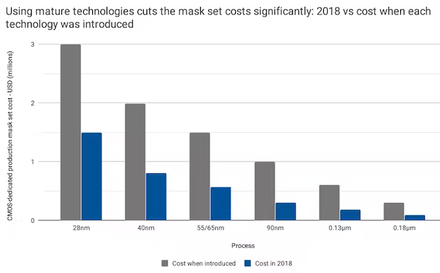
Graph © EnSilica plc, reproduced with permission
This shows the conundrum pretty clearly. Initially, mask prices were high enough to pay for capacity, but then they’ve dropped over the years. Now if we need more capacity, what are we going to do?
Let’s see:
- A mask vendor could buy more equipment, but it’s very expensive — Toppan mentioned \$65M for a new production line — and the return on investment isn’t economically viable, so they won’t buy more equipment.
- A mask vendor could charge more, to make it economically viable to buy more equipment, but then they would be charging more than their competitors, and lose business, so they won’t charge more.
- But if supply is limited, and customers can’t get the masks they need, shouldn’t the increased demand push prices up to the point where they can justify the investment in more capacity?
Something’s just wrong with this picture: either the economics is just broken, or I’m missing some subtlety. Maybe everybody believes the demand increase is temporary and they’re not willing to risk CapEx purchases that would increase their supply capacity. Perhaps this kind of belief only works at the leading edge, where there’s Moore’s Law and roadmaps — and a lot more profit.
I guess the takeaway is not to get our hopes up.
And, of course, realize that the choice of technology node to use in an IC can be a real fuzzy one, depending on engineering constraints, economic profitability, and future supply availability, in what seems right now to be a somewhat unreliable world.
Notes
Click here to skip ahead to the last section.
[37] Anton Shilov, TSMC to Customers: It’s Time to Stop Using Older Nodes and Move to 28nm, AnandTech, Jun 29 2022.
[38] Mark Bohr, Moore’s Law Leadership, Intel Technology and Manufacturing Day, Mar 28 2017. The extra “hyper scaling” tricks include Contact Over Active Gate (metal contact can be placed over a FinFET gate rather than next to it) and Single Dummy Gate (better process control to decrease the number of dummy gates that are required between transistors) — see Kaizad Mistry, 10nm Technology Leadership, Intel Technology and Manufacturing Day, Mar 28 2017.
[39] Scotten Jones, LithoVision – Economics in the 3D Era, semiwiki.com, Mar 4 2020.
[40] Scotten Jones, Technology and Cost Trends at Advanced Nodes, IC Knowledge, presented at SEMICON West, Jul 13 2016.
[41] EUROPRACTICE, TSMC 0.13 µm - 90, 65, 40, 28 & 16 nm PROTOTYPING AND VOLUME PRODUCTION (brochure), Sep 16 2022.
[42] Automotive Electronics Council, Fundamentals of AEC-Q100: What “Automotive Qualified” Really Means, Monolithic Power Systems, Nov 2018.
[43] Richard Oshiro, Failure Mechanism Based Stress Test Qualification for Integrated Circuits (AEC Q100 Rev G), May 14 2007. AEC Q100 Grade 1 is -40°C to +125°C, Grade 2 is -40°C to +105°C, Grade 3 is -40°C to +85°C (the old “I”-for-industrial temperature range of the CIM era), and Grade 4 is 0 to +70°C, equivalent to commercial temperature specifications.
[44] Barry Pangrle and Shekhar Kapoor, Managing leakage power at 90 nm and below, EE Times, Nov 5 2004.
[45] Gervais Fong, Low Power USB 2.0 PHY IP for High-Volume Consumer Applications.
[46] Gartner, Inc., Gartner Says Worldwide Smartphone Sales Declined 5% in Fourth Quarter of 2020, Feb 22 2021.
[47] Chipworks Inc., Apple iPhone 5 - the A6 Application Processor, Sep 21, 2012.
[48] TechInsights Inc., Apple iPhone 13 Pro Teardown Analysis, Sep 25, 2021.
[49] Joel Hruska, Apple unveils New A15 Bionic SoC, ExtremeTech, Sep 15 2021.
[50] Norio Matsumoto, iPhone 14 teardown reveals parts 20% costlier than previous model, Nikkei Asia, Oct 7 2022.
[51] Samuel K. Moore, A Better Way To Measure Progress In Semiconductors, IEEE Spectrum, 21 Jul 2020.
[52] Barry Pangrle, A Node By Any Other Name, Semiconductor Engineering, May 12 2014.
[53] Mark Richards, What to Expect at 5-nm-and-Beyond and What that Means for EDA, EE Times, Mar 14 2018.
[54] Ali Khakifirooz, CMOS Density Scaling and the CPP×MxP Metric, Aug 18 2015.
[55] Bill Arnold, Shrinking Possibilities, IEEE Spectrum, 1 Apr 2009.
[56] Intel submits technical papers to the IEEE International Electron Devices Meeting (IEDM) documenting many of their process technologies. Rather than giving individual footnotes, here they are as a group:
- 350nm: M. Bohr et al., A high performance 0.35 µm logic technology for 3.3 V and 2.5 V operation, Proceedings of 1994 IEEE International Electron Devices Meeting, 1994, pp. 273-276. (Note: MMP and CPP not given.)
- 250nm: M. Bohr et al., A high performance 0.25 µm logic technology optimized for 1.8 V operation, International Electron Devices Meeting. Technical Digest, 1996, pp. 847-850.
- 180nm: S. Yang et al., A high performance 180 nm generation logic technology, International Electron Devices Meeting 1998. Technical Digest (Cat. No.98CH36217), 1998, pp. 197-200.
- 130nm: S. Tyagi et al., A 130 nm generation logic technology featuring 70 nm transistors, dual Vt transistors and 6 layers of Cu interconnects, International Electron Devices Meeting 2000. Technical Digest. IEDM (Cat. No.00CH37138), 2000, pp. 567-570.
- 90nm: S. Thompson et al., A 90 nm logic technology featuring 50 nm strained silicon channel transistors, 7 layers of Cu interconnects, low k ILD, and 1 µm² SRAM cell, Digest. International Electron Devices Meeting, 2002, pp. 61-64.
- 65nm: P. Bai et al., A 65nm logic technology featuring 35nm gate lengths, enhanced channel strain, 8 Cu interconnect layers, low-k ILD and 0.57 µm² SRAM cell, IEDM Technical Digest. IEEE International Electron Devices Meeting, 2004., 2004, pp. 657-660.
- 45nm: K. Mistry et al., A 45nm Logic Technology with High-k+Metal Gate Transistors, Strained Silicon, 9 Cu Interconnect Layers, 193nm Dry Patterning, and 100% Pb-free Packaging, 2007 IEEE International Electron Devices Meeting, 2007, pp. 247-250.
- 32nm: P. Packan et al., High performance 32nm logic technology featuring 2nd generation high-k + metal gate transistors, 2009 IEEE International Electron Devices Meeting (IEDM), 2009, pp. 1-4.
- 22nm: C. Auth et al., A 22nm high performance and low-power CMOS technology featuring fully-depleted tri-gate transistors, self-aligned contacts and high density MIM capacitors, 2012 Symposium on VLSI Technology (VLSIT), 2012, pp. 131-132.
- 14nm: S. Natarajan et al., A 14nm logic technology featuring 2nd-generation FinFET, air-gapped interconnects, self-aligned double patterning and a 0.0588 µm² SRAM cell size, 2014 IEEE International Electron Devices Meeting, 2014, pp. 3.7.1-3.7.3.
- 10nm: C. Auth et al., A 10nm high performance and low-power CMOS technology featuring 3rd generation FinFET transistors, Self-Aligned Quad Patterning, contact over active gate and cobalt local interconnects, 2017 IEEE International Electron Devices Meeting (IEDM), 2017, pp. 29.1.1-29.1.4. Note: this paper doesn’t mention gate length, but two meeting attendees did note a minimum gate length of 18nm:
- Dick James, IEDM 2017: Intel’s 10nm Platform Process, Solid State Technology, Dec 18 2017.
- Scotten Jones, IEDM 2017 – Intel Versus GLOBALFOUNDRIES at the Leading Edge, semiwiki.com, Dec 22 2017.
- 7nm: Here it gets tricky; Intel recently renamed their 10nm and 7nm nodes as “Intel 7” and “Intel 4” to match competitiveness with other foundries having similar process characteristics. There is a paper on “Intel 4” (which would have been called 7nm): B. Sell et al., Intel 4 CMOS Technology Featuring Advanced FinFET Transistors optimized for High Density and High-Performance Computing, 2022 IEEE Symposium on VLSI Technology and Circuits (VLSI Technology and Circuits), 2022, pp. 282-283. I’m using Scotten Jones’s numbers for this node instead.
[57] Mark Bohr, Continuing Moore’s Law, Intel Technology and Manufacturing Day, Sep 19 2017. See slide 17 for transistor densities.
[58] Scotten Jones, ISS 2021 – Scotten W. Jones – Logic Leadership in the PPAC era, semiwiki.com, Jan 15 2021.
[59] Integrated Circuit Engineering Corporation, Section 7: Changing Wafer Size and the Move to 300mm, Cost Effective IC Manufacturing 1998-1999: Profitability in the Semiconductor Industry, 1997.
[60] IC Insights, Global Wafer Capacity 2021-2025 brochure, 2021. Table cites 1.3M MWC for ≤ 150mm, vs. 20.8M MWC total = 6.25%, where MWC = installed monthly capacity in 200mm-equivalent wafers)
[61] Scotten Jones, A Simulation Study Of 450mm Wafer Fabrication Costs, IC Knowledge LLC, presented Nov 2010.
[62] Trefis Team, Why Texas Instruments Is Expanding Its 300-mm Analog Capacity, Forbes, Dec 3 2018.
[63] Scotten Jones, The Lost Opportunity for 450mm, SemiWiki, Apr 15 2022.
[64] Design & Reuse, 300mm Capacity Dominates, but Life Remains for 200mm Wafer Fabs, Feb 6 2014.
[65] Scotten Jones, SEMICON Update: 450mm, EUV, FinFET, and More, SemiWiki, Jul 19 2014.
[66] David Lammers, Demand for 200mm Tools Outstrips Supply, Applied Materials Nanochip Fab Solutions, Jul 2015.
[67] Paul McLellan, 200mm Fabs Awaken, Breakfast Bytes, Jul 21 2016.
[68] Christian Dieseldorff, Watch Out For 200mm Fabs: Fab Outlook To 2020, Semiconductor Engineering, Oct 24 2016.
[69] Mark LaPedus, 200mm Crisis?, Semiconductor Engineering, May 18 2017.
[70] Ed Sperling, The 200mm Equipment Scramble, Semiconductor Engineering, Aug 23 2017.
[71] Christian Dieseldorff, 200mm Fabs Still Flexing Muscles, Semicon Europa, Nov 14-17 2017.
[72] Mark LaPedus, 200mm Fab Crunch, Semiconductor Engineering, May 21 2018.
[73] Christian Dieseldorff, 200mm Fabs Add 600,000 Wafers Per Month — Is There an End in Sight?, Jul 19 2018.
[74] Mark LaPedus, Demand Picks Up For 200mm, Semiconductor Engineering, Feb 20 2020.
[75] Mark LaPedus, 200mm Shortages May Persist For Years, Semiconductor Engineering, Jan 20 2022.
[76] Adele Hars, Wafer Shortage Improvement In Sight For 300mm, But Not 200mm, Semiconductor Engineering, May 19 2022.
[77] David Anderson, Stoking the productivity engine with new materials and larger wafers, Solid State Technology, Mar 1997.
[78] Yoichiro Hiroi, China hoards used chipmaking machines to resist US pressure, Nikkei Asia, Feb 28 2021.
[79] SPG Media Limited, Texas Instruments DMOS6 300MM Expansion, Dallas, TX, USA, semiconductor-technology.com, uploaded sometime in May 2004.
[80] TSMC 2014 Q4 earnings call, Jan 15 2015.
[81] TSMC 2010 Q3 earnings call, Oct 28 2010.
[82] TSMC 2013 Q2 earnings call, Jul 18 2013.
[83] TSMC 2022 Q1 earnings call, Apr 14 2022.
[84] TSMC 2022 Q3 earnings call, Oct 13 2022.
[85] TSMC, Consolidated Financial Statements for the Six Months Ended June 30, 2022 and 2021 and Independent Auditors’ Review Report, Aug 9 2022. See also Tom’s Hardware, TSMC Collects Huge Prepayments, Nov 17 2021.
[86] Anton Shilov, TSMC to Expand Capacity for Mature and Specialty Nodes by 50%, AnandTech, Jun 16 2022.
[87] TSMC 2021 Q4 earnings call, Jan 13 2022.
[88] TSMC press release, TSMC to Build Specialty Technology Fab in Japan with Sony Semiconductor Solutions as Minority Shareholder, Nov 9 2021.
[89] Vladimir Koifman, TSMC Builds a Dedicated 28nm Fab for Sony Orders, Image Sensors World, Jul 6 2020.
[90] Tom Dillinger, TSMC 2022 Technology Symposium Review – Process Technology Development, SemiWiki.com, Jun 22 2022, original text captured on archive.org.
[91] Mark LaPedus, Photomask Shortages Grow At Mature Nodes, Semiconductor Engineering, Apr 21 2022.
[92] International Technology Roadmap for Semiconductors, Lithography, 2007. (Mentions 33 mask levels for MPU for 68nm half-pitch.)
[93] Jack Chen, The Challenges of Lithography, NanoPatterning Technology Co., Mar 1 2019. (Includes graph with approx 32-33 masks at 90nm, 37-38 masks at 65nm, 45-46 masks at 40nm, 50-51 masks at 28nm.)
[94] Ian Lankshear, The Economics of ASICs: At What Point Does a Custom SoC Become Viable?, Electronic Design, Jul 15 2019.
We Can Work It Out: The Fab Four Supply Chain (Through the Looking Glass)
There’s certainly a lot to learn about the economics of semiconductor manufacturing. I’ll leave you with one more topic today, and that is the supply chain itself. None of the companies we’ve talked about exists in a vacuum; each has its own customers and suppliers, forming a complex economic network we think of as the supply chain. An extreme event like the 2021 semiconductor shortage can motivate the actors in that supply chain to rethink their relationships. There is undoubtably a lot of “what if” going on in the industry.
We’ll engage in some “what if” of our own, and look at four hypothetical companies in a fictional supply chain. (In part this is so we can be creative and become free of the constraints of the real world, and in part it’s just to have some fun.)
Here they are:
Company Description 
Frob Motor Company
One of the world's largest and oldest automobile manufacturers, now diversifying into electric vehicles. From a well-known ad campaign: Have you recently operated a Frob? Corporate logo very popular, known as the Nauseous Green Parallelogram.

Earl Corporation
A large Tier 1 supplier to several automotive OEMs, specializing in electronic automotive systems.

Kansas Instruments, Incorporated
A diversified manufacturer of semiconductors and integrated circuits, headquartered in Lawrence, Kansas. Colloquially known as "KI".

Huang Zhong Manufacturing Corporation
HZMC is a major pure-play semiconductor foundry, and supplies finished wafers to most major semiconductor manufacturers.
Our view of the supply chain for an IC produced by a fabless or fab-lite semiconductor vendor looks like this, which I’ll call the “Auto Fab Four” supply chain:

Kind of boring. KI designs ICs and has them manufactured at a foundry, HZMC. Then KI’s chips get designed and manufactured in a subsystem by Earl, a Tier 1 supplier. Earl then sells this subsystem to Frob as a critical component in its cars and trucks, which Frob sells all over the world.
There are several alternatives worth pointing out:
-
The Integrated Device Manufacturer (IDM) — this is when a foundry isn’t part of the chain. For some chips, notably ones that are manufactured on mature nodes, KI designs and manufactures in-house, then sells them to Earl for subsystems, which Frob purchases and puts into its cars and trucks.

-
The Diversified Fabless Subsystem Manufacturer — occurs when a fabless semiconductor manufacturer integrates upwards into subsystem designs, or a subsystem designer gets into the IC design business.


-
The Fabless Chip-Design-Savvy Systems Integrator (“OEM-Foundry-Direct”) — recently, some large companies have had cases where it makes sense for them to design ICs directly and work with a foundry to manufacture them. Examples include Amazon, Apple, Google, Microsoft, and Tesla.[95] Gartner put out a press release last December predicting that many of the top automotive manufacturers would join this category and design their own chips.[96]

-
Real Tier Ones Have Fabs — some automotive suppliers find it economically valuable to run their own semiconductor fabs. In the distant past, Motorola would have been in this category, with their production of transistor car radios. Bosch operates its own fab, and Denso has invested in TSMC’s Kumamoto fab.

-
The Vertically-Integrated OEM. Not particularly common nowadays; in the past, this included IBM (in computers) and Commodore (in calculators and computers, after purchasing MOS Technology) and General Motors, which operated a semiconductor plant in Kokomo, Indiana, until 2017. [97]

How did we get to the “Auto Fab Four” supply chain?
Remember, fabs are an enormous capital expense. Foundries, which can reach high enough volumes and utilization of their fabs to take advantage of the economies of scale, are now very difficult to beat for cost effectiveness. They spend all their R&D on how to become better in leading-edge node manufacturing, and have become extremely cost-effective on trailing-node manufacturing, where the fab equipment has been fully depreciated. An IDM doesn’t have the economy of scale of large foundries to warrant that kind of R&D expenditure and operational efficiency. In our through-the-looking-glass supply chain, this means that in some cases Kansas Instruments finds it more cost-effective to outsource production to the HZMC foundry, than to try to run a leading-edge fab, which would tie up capital costs that KI could otherwise spend on its own R&D. So we now have very large specialist foundry firms.
Similarly on the IC design front — chip design is expensive, so we now have very large specialist chip design firms, that can leverage economies of scale and put their R&D funds into becoming more competitive chip designers. KI can design microcontrollers with very high expected volumes, and has the benefit of R&D experience designing many different ICs based around similar architectures. For subsystem manufacturer Earl, the volumes aren’t sufficient to maintain a dedicated IC design department.
Economic specialization leads these semiconductor firms to a competitive edge — also known as an “economic moat” — in an industry with high barriers to entry, where that competitive edge is honed by competing for business from a large customer base. (I’m not as familiar with the “Tier 1” automotive supplier system, but I’d imagine this same moat/barriers-to-entry/large-customer-base issue is the reason there are Tier 1 suppliers, and the reason Frob Motor Company purchases subsystems from those suppliers rather than trying to design and manufacture its own circuit boards.)
The high CapEx and technology R&D cost factors tend to reward this kind of specialization; for example, a new firm raising capital to enter the semiconductor market and sell new ICs will almost certainly be fabless, because of the lower barrier to entry. There are other factors, however. Supply risk and quality control drive the other direction, towards vertical integration: a company that is its own captive supplier can (in theory) do a better job assuring internal supply and quality.
One big factor that is really hard to get a definitive answer is profitability. Is it really more profitable to outsource semiconductor manufacturing? This is not a trivial question. Forget everything else, about supply risk or quality or CapEx or technological competitiveness, and let’s just think about profitability.
I’ll give you a hint: many industry statements on the fabless / IDM debate are misleading, because they’re answering the wrong question. The noticeable differences pointed out have correlation with other factors besides the choice of fabless/IDM.
- “Fabless companies have a more profitable cost structure than IDMs”[98] — compares financial profitability from sets of companies with different market segments
- “Fabless was the best performer during this period [2013 - 2017], with memory in second place.”[99] — measures economic profit, dependent on differences in market size
- “Thirty-nine companies reported a Q1 2012 net profit margin higher than the 12.1% average. 92.3% of these companies were fabless.”[100] — compares net profit margin of various companies of different size, age, and market segments… and aren’t there more fabless semiconductor firms than IDMs, anyway?
We can’t compare firms without correcting for these other correlations, but I don’t feel confident with the required level of statistical analysis.[101] Instead, let’s engage in a thought experiment, about the choice that a particular firm has on one project, and whether to outsource or not.
HHG Profitability Analysis
Here’s an example:
Let’s suppose Kansas Instruments is thinking about its next project, the KMS990 microcontroller series, on 65nm silicon. It has a 300mm fab, and can, in theory, expand capacity to support the KMS990 in-house. It is also considering having the KMS990 manufactured at HZMC, who offers KI a price per wafer that works out to be \$1.00 per die. Internally to HZMC, this works out roughly as follows:
(NOTE: These are made-up numbers intended to be in the same ballpark as the corresponding numbers from real-world companies.[102] I believe they are realistic enough for a horseshoes-and-hand-grenades profitability analysis. They may be off by 10-20% — the intent is not for them to be perfectly accurate, but rather to get a point across. There is low sensitivity to errors in most of my estimates: in other words, try changing these numbers and you’ll still find the same sort of takeaways.)
- 35 cents per die: cost of goods sold (equipment depreciation, raw materials, chemicals, electricity and water costs of the fab, and labor expenses directly involved in manufacturing)
- 10 cents per die: allocated to the company’s operating expenses (R&D, general and administrative expenses, marketing costs)
- 6 cents per die: taxes, approx 10% of income before taxes
- 49 cents per die: net profit
How can we compare this against the possibility of KI manufacturing this microcontroller internally?
If KI makes the KMS990 in-house, there are three types of expenses it doesn’t need to cover:
- HZMC’s net profit (49 cents)
- HZMC’s income taxes (6 cents)
- Transaction costs that would be involved in HZMC’s sale of wafers — let’s just guesstimate 1 cent per die for this — from the following sources:
- An appropriate portion of HZMC’s marketing expenses to help sell its foundry services (0.5 cent per die)
- Contract costs for the KMS990 borne by HZMC — including business and legal staff to negotiate a contract, and finance staff to execute a contract (0.25 cent per die)
- Contract costs for the KMS990 borne by KI (0.25 cent per die)
(Note: my understanding of economics is very rough, so I may well have missed something important here. If you wish to ponder the role of transaction costs, Coase’s classic paper, The Nature of the Firm[103] is a relatively easy place to start.)
There’s also one expense that KI does need to cover if it manufactures the KMS990 in-house, which is the project’s share of KI’s opportunity cost of capital for owning and operating a semiconductor fab. This is a fuzzy one to explain, let alone estimate a value, since I don’t know how it shows up in corporate balance sheets. I’ll give a shot at an explanation, and hope that I get it right.
Let’s say that it would cost exactly the same for KI to manufacture wafers of a number of chips like the KMS990 in one of its own fabs, as it would to have them made at a foundry like Huang Zhong. We include all the accounting costs here, so the depreciation of the fab equipment and the upkeep of the building and the labor costs of running the fab — that’s all included. And management decides that there is no net financial impact on the business between continuing to operate this fab, as it is to not operate it; everything balances out, supply risk and CapEx and what-have-you. Except for one fact: KI could sell the fab, including all the equipment, say, for a billion dollars, and use that billion dollars to invest in other areas of R&D instead, to improve the return on its business.
This means there is economic cost just to own an asset, where its value could be used for other purposes. (Online sources to calculate Weighted Average Cost of Capital seem to show about 10% for semiconductor companies — for example, NXP’s 2012 annual report[104] mentions WACC in the 10.5% - 13.7% for its business units and an overall average WACC of 12.4% — so a billion dollars sunk into a fab would have to yield about \$100 million each year in extra return to justify the cost of keeping the fab as an asset. I don’t understand the WACC calculation, so can’t comment on whether 10% is about right; YMMV.)
If Kansas Instruments sees that HZMC is a reliable foundry partner, and can assure KI a reliable supply of chips, for about the same cost, then it may well decide to sell its own fab, and put the money to better uses. (Which is one big financial reason that some semiconductor companies have gone fabless.) But in times like this chip shortage, the opportunity cost of capital for owning a fab may actually swing negative: even if it costs more to make its chips in-house, the assurance of a supply source it can control is worth that extra cost.
Okay — I have no idea how to guess at an opportunity cost of capital that could be allocated to each die, so I’m just going to guess 10 cents per die. (As 10% of the total cost to fabricate the die, and 6.8% of the total COGS, this seems in the right ballpark[105] — but accuracy doesn’t matter that much; in the cost breakdown below, feel free to replace 10 cents with any number \( x \) between 0 - 20 cents and 81 cents with \( 91 - x \) cents, and you get the same general conclusion.)
KI can get away a higher manufacturing cost for the KMS990 in-house, with the following as a break-even profitability with buying from HZMC:
- 81 cents per die: cost of goods sold
- 9.25 cents per die: allocated to the company’s operating expenses for manufacturing KMS990 die
- 10 cents per die: opportunity cost of capital to run the fab
- -0.25 cents per die “rebate” from what KI does not have to incur in operating expenses for foundry contract costs
The term break-even here refers to the decision of outsourcing based on whether KI’s total manufacturing costs at its own fabs for finished wafers would be lower or higher than the \$1.00 per die it can pay to HZMC to do the same thing:
- significantly higher than \$1.00 per die → KI should probably outsource instead
- significantly lower than \$1.00 per die → KI should probably use internal fabs
- about the same → make a decision based on other factors
In this estimated analysis, KI’s COGS can be over twice as high as HZMC’s COGS and still justify making chips in-house. In other words, KI doesn’t need to be as economically competitive as the foundry! Which is a good thing, because it also is unlikely to be as efficient as the foundry: KI’s fabs are captive fabs for its own products, and are only one piece of the business, whereas as a foundry HZMC does one thing extremely well: manufacture finished wafers, competing with a handful of other companies to do so.
This might just seem like a jumble of numbers, so here’s the same information in graphical form:

The top two bars are the die cost breakdown for HZMC and KI — assuming it can meet the same \$1 die cost. Again: the pink opex “rebate” for KI’s die cost is operating expenses that don’t have to be paid because KI doesn’t have to cover business/legal/finance costs for in-house IC manufacturing which it would have to pay to negotiate and execute a contract with the foundry.
We can go through the same kind of HHG estimate for KI’s profitability[106], which is shown in the bottom bar of the graph above.
- Revenue:
- \$3.25 per IC
- Costs:
- COGS: (45% of revenue, 55% gross margin)
- Operating expenses:
- \$1.00 per IC (31% operating expenses due to IC design, applications engineering, marketing, sales & administrative costs)
- Operating profit: 78.5 cents per IC (24% operating margin)
- Taxes: 7.8 cents (10% effective tax rate)
- Net profit: 70.7 cents
If KI does a good job understanding its customer requirements and demand, the KMS990 might be a best-seller, and the operating expenses over the manufacturing life of this chip might be a much lower percentage of revenue. Or it might be a flop, and KI’s profit disappears.
Again, please note: these are not real numbers, but I believe they are realistic enough. Some semiconductor firms might have 5% operating margin and others 40% operating margin. It doesn’t matter that much; the same economic issues apply when they decide whether to operate their own wafer fabs or outsource to a foundry.
Our Tier 1 supplier, Earl, could make the same kind of profitability tradeoff: continue to buy the KMS990 from KI, or design its own MCU and have it fabricated at HZMC. Earl’s differences in profitability would be roughly as follows:
- Less expense from not having to pay for KI’s IC profit and tax expenses
- More expense in operating expenses to design the IC, because Earl does not have staff who are as experienced and competitive as KI’s designers
- More expense in packaging, because Earl would likely have to outsource to a different vendor that can’t handle assembly as efficiently as KI
Only the very largest of Tier 1 suppliers that do a lot of business in electronic subsystems would be able to justify an in-house IC design.
Finally, Frob Motor Company could cut out its supplier in this case (Earl), but this seems unlikely to happen; I found one study stating that the operating margins of Tier 1 auto suppliers are in the 6-8% range,[109], so there doesn’t seem like much profitability benefit.
Real world: fab-lite or fabless?
In the real world, there’s been a mix of supply chain choices.
Nearly all of the automotive and industrial semiconductor manufacturers are fab-lite, with wafer production split between internal and external fabs. Others in the consumer or microprocessor space (Qualcomm, Broadcom, Marvell, AMD, Nvidia, MediaTek, etc.) are fabless. While profitability and technology node choice may be part of the reason — consumer microprocessors or SoCs are more likely to require leading-edge nodes, where it’s too costly to compete against the foundries — this combination is not the only factor. Perhaps the shorter market lifetime is another reason for to pursue fabless operation. The automotive/industrial market needs ICs to stay in production for a long time — NXP’s “Product Longevity” program guarantees a minimum of fifteen years for some automotive, telecommunications, and medical ICs — so supply chain risk mitigation is probably just as much of a concern.
In an analysis of the fabless/IDM choice, Rahul Kapoor noted some additional reasons for firms to use a mix of both internal and external production:[101]
For example, firms have been shown to pursue both make and buy so as to gain flexibility and manage industry volatility, improve their bargaining power over external suppliers, and leverage theirs and suppliers’ differential capabilities.
This seems to match some of the strategic reasons that Texas Instruments chose to use both internal and external production:
-
In 2006 it was to counteract the foundries’ ability to exert monopoly/oligopoly pricing pressure:[110]
TI’s high-volume customers in the cell phone business see the benefits of getting products from multiple fabs, Miller said. For the 65-nm generation, for example, TI expects to source chips from seven fabs. Thus, “our customers are not totally exposed to any one fab. Even though some parts may be made only in a foundry, that is not a huge issue for them now,” he said.
The Richardson fab is part of the “insurance policy” TI needs to keep foundry pricing within certain parameters. With Richardson ready to be equipped, the foundries know that TI’s ability to pull more manufacturing in-house is only 15 months away, Miller said.
-
In 2007 it was more of an “if you can’t beat ’em, join ’em” approach, where TI essentially admitted the foundries could develop leading-edge technology nodes better, and partnered with them to develop a 32nm process:[111]
At 32 nm, TI plans to bring its hybrid strategy to new heights. In the past, process development efforts required three distinct R&D activities. TI developed its own process; foundry partners independently did the same. A third R&D effort brought the separate processes into the production phase.
Starting at the 32-nm node, TI and its foundry partners will jointly work on process technology. The process will be defined and developed at the foundry, instead of within TI, and then be “copied” and transferred or fanned back to TI’s own fabs. In a sense, that will make TI’s fabs complementary to the foundries, VLSI Research’s Lammers said.
Even as it shifts responsibilities to the foundries for digital processes, TI is investing in its own analog processes and fabs — and for good reason. Nearly half of the company’s total sales revolve around analog, and the fragmented sector is growing faster than the overall semiconductor industry, said Art George, senior vice president of high-performance analog at the company.
Customers of the semiconductor manufacturers are also making strategic choices. The foundry and semiconductor design steps are not guaranteed places in the supply chain. The severe stress that the chip shortage has been placing on the automotive industry has made for some creative thinking. Recently the idea of “partnerships” seems to be floating around, with the automotive companies getting involved more directly somehow with chip designs, even if they don’t actually do the designs themselves. In November 2021, GM announced plans for a semiconductor partnership with Qualcomm, ST, TSMC, Renesas, ON Semi, NXP, and Infineon:[112]
General Motors plans to launch a strategy that will reduce the number of unique microcontroller units required by 95 percent in order to streamline hardware and software advancements and secure its semiconductor supply chain, GM President Mark Reuss said Thursday.
Under the strategy, hardware and software developers will draw from three families of chips, put together by partnerships between GM and various suppliers, Reuss said during Barclays Global Automotive and Mobility Tech Conference. The plan will help the automaker meet its goal to double revenue by 2030 and could strengthen GM’s flow of semiconductors after the global microchip shortage pummeled vehicle production industrywide this year.
GM expects semiconductor requirements to more than double over the next several years. It will consolidate core microprocessor chip purchases into three families co-developed, sourced and built with leading semiconductor manufacturers. The strategy is designed to support electric vehicle, autonomous vehicle and connected services growth, Reuss said.
“This will drive quality and predictability. Even one of those families of the three could alone account for more than 10 million units annually,” Reuss said. “Those three core microcontrollers are really designed to provide more than seven years of platform stability, so that really unlocks software developers to focus on the creation of high-value customer-facing future content within the company.”
Stellantis announced a similar partnership with Foxconn in December 2021:[110]
“Our software-defined transformation will be powered by great partners across industries and expertise,” said Carlos Tavares, Stellantis CEO. “With Foxconn, we aim to create four new families of chips that will cover over 80% of our semiconductor needs, helping to significantly modernize our components, reduce complexity, and simplify the supply chain. This will also boost our ability to innovate faster and build products and services at a rapid pace.”
Other partnerships announced within the last year include Volkswagen and Qualcomm,[113] Ford and GlobalFoundries, BMW and Inova and GlobalFoundries, GM and Wolfspeed,[114] and DENSO and foundry UMC’s subsidiary USJC.[115]
Will these sorts of partnerships actually help improve profitability and/or supply assurance? We’ll all just have to wait and see.
Notes
[95] James Morra, Technology Giants to Step Up Chip Design Ambitions in 2022, Electronic Design, Jan 11 2022.
[96] Gartner Inc., Gartner Predicts Chip Shortages Will Drive 50% of the Top 10 Automotive OEMs to Design Their Own Chips by 2025 (press release), Dec 7 2021.
[97] Joseph Szczesny, GM Closing Indiana Semiconductor Plant, The Detroit Bureau, Nov 30 2016.
[98] Jeremy Wang, Global Fabless/Foundry Collaboration and Innovation, Fabless Semiconductor Association, Aug 15 2007. Compares median 2005 earnings before taxes and amortization from a set of IDM firms (TI, ST, Infineon, Hynix, AMD, Freescale, NEC EL, Micron, Qimonda, Rohm, ADI, Vishay, National Semiconductor, Elpida) and fabless firms (Broadcom, nVidia, SanDisk, ATI, Xilinx, Marvell, MediaTek, Altera, Sunplus, Novatek, Conexant, Via, Qlogic, Omnivision).
[99] Marc de Jong and Anurag Srivastava, What’s next for semiconductor profits and value creation?, McKinsey on Semiconductors, Oct 2019. Cites \$77.6B economic profit from “fabless” (Broadcomm, Qualcomm, Apple) vs. \$27.0B economic profit from “diversified IDM” (TI, Toshiba, NXP)
[100] Design & Reuse, GSA Announces the Fabless Sector Outperforms the Overall Industry in the First Quarter, Jun 29 2012.
[101] Rahul Kapoor, Persistence of Integration in the Face of Specialization: How Firms Navigated the Winds of Disintegration and Shaped the Architecture of the Semiconductor Industry, Wharton School, University of Pennsylvania, Sep 9 2011. Kapoor ran a least-squares linear regression of Return on Invested Capital (ROIC) against various factors for semiconductor firms from 1993 - 2007. Fabless firms had an increase in the mean ROIC of 0.7% with a standard error of 6.6%, which is not statistically significant. Statistically significant factors were firm size (larger revenue had higher ROIC), firm age (newer firms had slightly higher ROIC), industry revenue growth (higher growth had higher ROIC), and whether the firm was Taiwanese (higher ROIC).
[102] TSMC’s 2022Q2 consolidated statement is worth looking at in detail; cost of revenue was 41% with a gross profit margin of 59%. Depreciation recognized in cost of revenue (over 93.5% of total depreciation; most of the rest was recognized as operating expenses) was 47.5% of the cost of revenue and is likely wafer fab equipment depreciation, with the bulk of it likely from the advanced nodes (5nm and 7nm) that made up 45.6% of TSMC’s total revenue in this quarter. The advanced nodes are likely to see lower gross margin and the mature nodes likely to see higher gross margin; a split of 45% gross margin for advanced nodes and 70% gross margin for mature nodes is quite possible. Recent quarters may have higher-than-normal profitability because of the chip shortage, so I wouldn’t expect them to stay this high forever. TSMC’s exact profitability metrics per node are proprietary and are not published, of course.
TSMC also has had operating expenses at about 10.5-11% of revenue, with about 8% of it going to research and development, about 2% going to general and administrative costs, and about 0.4 - 0.5% going to marketing costs.
[103] Ronald H. Coase, The Nature of the Firm, Economica, Nov 1937.
[104] NXP Semiconductors N.V., Annual Report for the Financial Year Ended December 31, 2012, dated May 1 2013.
[105] Just as some examples:
-
NXP’s 2012 annual report states that cost of revenue was \$2.355 billion (page 60); property, plant, and equipment value (less depreciation) was \$1.078 billion (page 103); and WACC was 12.4% (page 130). WACC * PPE value = \$134 million which is about 5.7% of the cost of revenue. In October 2012, NXP reported using foundries for 15% of chip production, on 90nm and 40nm processes, intending to expand to 35% of production in 2015 — which is why I’m using an older annual report rather than a current report, so it doesn’t overstate the cost of revenue.
-
Texas Instruments’ 2003 annual report states that the cost of revenue in 2002 was \$5.313 billion (page 27) and property, plant, and equipment value (less depreciation) was \$4.794 billion (page 28). 10% of PPE value = \$479 million = approximately 9% of the cost of revenue. (In February 2002, TI reported outsourcing about 5% of production to foundries.)
-
ON Semiconductor’s 2020 annual report mentions a discount rate of 12.0% (page 104) for in-process research and development (IPRD), cost of revenue of \$3.539 billion (page 54), property, plant and equipment value (less depreciation) of \$2.512 billion (page 116), and states that third-party contractors accounted for 33% of total manufacturing input costs (page 20). The cost of revenue not from outsourcing would be 100-33% = 67% of cost of revenue = \$2.37 billion; discount rate * PPE = \$301 million = 12.7% of internal cost of revenue.
These calculations probably overstate opportunity cost of capital for fabs, given that the fabs are only part of total property/plant/equipment value — these companies do have headquarters and R&D facilities.
[106] I picked these numbers as being in roughly the same ballpark as the consolidated income statements from the years listed in the latest annual report (2021 or 2022) for these fab-lite semiconductor companies serving the automotive and industrial markets: Analog Devices, Diodes Incorporated, Infineon, Microchip Technology, NXP, ON Semiconductor, Renesas, ST Microelectronics, and Texas Instruments.
[107] AnySilicon’s website told me that a 64-pin 9x9 QFN at high volume is estimated to cost 23 cents. I’ll take that as a HHG estimate if only because I have nothing better. And I guessed that the costs to run final IC tests at the end of the assembly process were about the same.
[108] Randy Schmidt, The back-end process: Step 9, Solid State Technology, Oct 2000. (“Desired yields from established assembly processes are typically greater than 99 percent; electrical fallout that can be attributed to assembly-related defects should run less than 0.5 percent.”) No idea how reasonable this is; 99% yield seems high.
[109] Automotive from Ultima Media, Tearing profits apart: how tier 1 automotive suppliers can mitigate shrinking margins, Jan 7 2020.
[110] Stellantis, Stellantis, Foxconn Partner to Design and Sell New Flexible Semiconductors for Automotive Industry, press release, Dec 7 2021.
[111] Mark LaPedus, TI takes two approaches to IC manufacturing, May 13 2007.
[112] Hannah Lutz, GM to work with leading semiconductor suppliers, Reuss says, Automotive News, Nov 18 2021.
[113] Reuters, VW embeds Qualcomm chips in autonomous driving software plans, May 3 2022.
[114] James Morra, GlobalFoundries Strikes Deal With BMW to Supply Scarce Chips, Dec 27 2021.
[115] DENSO Corporation, DENSO and USJC Collaborate on Automotive Power Semiconductors, news release, Apr 26 2022.
Wrapup
There are many takeaways from our continuing exploration of semiconductor economics. (Once again: I am not an economist, and not directly involved in semiconductor design or production — most of the raw material for this article is based on the crumbs of truth I found in publicly available sources — so if you happen to notice errors or oversights in this article, I welcome any feedback.)
-
Moore’s Law is really an economic strategy of emergent expectations within the semiconductor industry, to maintain a useful collective pace, like a flock of starlings, or a peloton of cyclists.
-
Roadmaps set by the major participants have allowed coordination of technological improvement, so that the individual firms don’t have to bear the risk of moving forward alone in the supply chain.
-
Transistor density has increased exponentially at a more-or-less regular pace.
-
Economies of scale have allowed the cost per transistor to drop exponentially, also at a more-or-less regular pace.
-
The coordinated pace of technology development allows semiconductor firms at all levels of industry (semiconductor equipment manufacturers, foundries, IDMs, fabless firms, EDA software vendors) to engage in competitive research and development, but also have some assurance their suppliers and customers will be ready to support their business when new products come to market.
-
Technology node names (180nm, 28nm, etc.) have diverged from a real-world measurement, and now are more of an abstract marketing concept. (See Myth #2.)
-
Remember the fine print in Moore’s original 1965 article: The complexity for minimum component costs has increased at a rate of roughly a factor of two per year. The pace of Moore’s Law has slowed, but the point is that technology advancements create an economy of scale that favors increasing the number of transistors, not necessarily the number of transistors for a given cost. As consumers, we like it when the total cost per chip stays the same, but even if cost-per-transistor improvements slow down, Moore’s Law is still likely to drive up the number of transistors in high-end applications.
-
-
Pure-play semiconductor foundries, starting with TSMC in 1987, originally filled a role to support small custom IC designers, and to provide extra capacity to large IDMs, at trailing-edge technology nodes. Since then, they have overtaken most IDMs, and have specialized in achieving leading-edge semiconductor production at very high volumes, to take advantage of economies of scale. They focus their competitive advantage on the fabrication process rather than trying to design and sell ICs.
-
Foundries earn their capital expenditures back on each new expensive fab in the first few years, by offering premium leading-edge technology, and after that, these fabs don’t go away; instead, they stay in production as these aging nodes become trailing-edge technology, with capacity and revenue that stays fairly steady. Remember the bell chord graphs:
-
The capacity available at the foundries evolves, presenting new less-expensive opportunities in technology nodes after semiconductor equipment has fully depreciated and the leading edge has moved on to the next node. I’ll try to annotate this on the 2011 McKinsey graph:
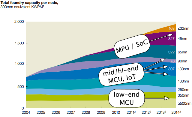
At the leading edge are high-volume microprocessors and system-on-chip (SoC) devices, and high-performance processors. Low-end MCUs stay where the manufacturing is cheap, and the mid-to-upper end of the MCU market has moved in to utilize capacity that’s no longer leading-edge, as the price per wafer on those nodes becomes more affordable.
-
We looked at the game Supply Chain Idle, where a fixed space of 20 plots of land allows production of various goods in factories, sometimes requiring other goods as input materials. The resulting income allows productivity upgrades to these factories to be more productive, or the conversion of these factories to produce more advanced and profitable goods.
-
Balancing the supply chain is important to prevent bottlenecks, where material piles up too fast to be used, or factory equipment is idle because input materials cannot be obtained fast enough. In either case, productivity is lowered.
-
Upgrades change the balance of the supply chain, sometimes motivating an abrupt shift to producing more profitable goods.
-
Small evolutionary upgrades are quicker than revolutionary changes in production, but can use up the capital needed for those revolutionary changes.
-
-
We looked at the Raspberry Pi RP2040, and some of the motivating factors that drove the RP2040 design team to choose 40-nanometer technology for the chip.
-
Smaller, lower-cost ICs, such as low-end microcontrollers, face economic and technological barriers that keep them on trailing-edge nodes. (See Myth #1.)
-
The economic barrier is that the up-front costs of the more advanced fab processes are too high for these manufacturers to recoup their investment, except at unattainable sales volumes.
-
The technological barrier involves constraints such as the need for nonvolatile memory, or the fact that some parts of the IC (I/O bond pads and drivers, and analog circuitry, for example) do not scale down at smaller technology nodes.
-
For the economic barrier, we went through some very rough (“horseshoes and hand grenades”) cost modeling to understand how the breakpoint between fixed up-front costs and per-unit costs is affected by the choice of technology node and die size.
-
This breakpoint is dependent mostly on the number of wafers purchased, so if Chip B is 100× smaller than Chip A produced on the same fab process, and both chips have the same up-front costs, then Chip B needs to sell 100× more volume than Chip A to have the same fraction of up-front costs. (Chip B’s development costs are very likely to be less than Chip A’s, but non-scalable factors, such as mask set costs, favor the profitability of the larger chip. There’s the fine print of Moore’s Law again: The complexity for minimum component costs has increased....)
-
-
Demand at these trailing-edge nodes has gone up consistently in the last 7-8 years, enough that there are severe 200mm wafer equipment shortages. (See Myth #3.)
-
300mm wafer fabs are more economically efficient than 200mm wafer fabs. (One estimate is 28% less expensive, another 40%; see Myth #3.) But the capital costs involved in building them are too high to justify except at leading-edge or near-leading-edge nodes.
-
300mm fab equipment doesn’t appear to exist for 180nm and older nodes; for these mature nodes we’re stuck with 200mm wafer equipment, where much of the used equipment has been snapped up already.
-
The older 300mm nodes — 130nm down to 40nm — are in this gray area where they don’t seem to be profitable enough to support the construction of new fabs. Fabs in this range of technology node were built when they were leading-edge nodes, and the foreseeable income stream was high enough to justify the cost. (See Myth #4.)
-
The only efforts to build new “mature node” fabs at the foundries appear to be at the 28nm node.
-
-
We looked at a fictional “auto fab four” supply chain with four participants, and considered some alternatives with fewer participants, along with profitability and other issues that might support or refute the viability of those alternatives.
The economics of the semiconductor industry is a harsh truth. Billions of dollars is on the line, and everyone wants the price of chips to keep coming down, but the equipment costs are so high that it makes for some frustrating economic realities. These have become apparent in recent months in the more mature nodes that are affecting our chip shortage, especially for automotive companies. One article I read — Semiconductor Engineering’s 2018 article Wanted: Mask Equipment For Mature Nodes — put it very succinctly, covering the lithography photomask industry:
Indeed, mask equipment vendors focus more of their attention on the leading edge, and not the trailing edge. The profits are higher at advanced nodes and the margins are slim for older systems.
Consequently, the industry is reluctant to build, upgrade and maintain older mask gear, which is coming back to bite the industry. Now, amid demand for trailing-edge masks, there is a shortfall of equipment in most of the major categories.
Thanks for reading!
In Part Four, we’ll look around at some current events and see how things have changed since the chip shortage began in late 2020.
Addenda
Further Reading
Here are a few other references worth reading:
-
John A. Mathews and Dong-Sung Cho, Tiger Technology: The Creation of a Semiconductor Industry in East Asia, 2000. A fascinating history of how Korea, Taiwan, Singapore, and Malaysia developed their semiconductor industries. Covers some of the early history of TSMC.
-
Eric Bogatin, Roadmaps of Packaging Technology: Driving Forces on Packaging: the IC, Integrated Circuit Engineering Corporation, 1997. A good quantitative summary of several aspects of Moore’s Law.
-
National Research Council, Dispelling the Manufacturing Myth: American Factories Can Compete in the Global Marketplace, 1992. Chapter 3 covers semiconductors and mentions captive suppliers.
-
National Research Council, Productivity and Cyclicality in Semiconductors: Trends, Implications, and Questions: Report of a Symposium, 2004. Good stuff here: Moore’s Law, SEMATECH, and foundries, oh my!
-
Dick James, A Trip Down TSMC Memory Lane — Part 1, TechInsights blog, Nov 15 2022. Good stuff if you like looking at electron microscopy images of chip cross-sections to see the layer stacks.
Acknowledgements
This article would not be possible without the assistance and encouragement of the following people: Ben Bayer, Antoine Bercovici, Randy Isaac, Brant Ivey, Ian Lankshear, John McMaster, Bill Mensch, Mark Richards, Ken Shirriff, and Jon Y.
© 2022 Jason M. Sachs, all rights reserved.