


VolksEEG Project: Initial Hardware Architecture
The initial hardware architecture for the prototype VolksEEG uses an Adafruit Feather nRF52840 Sense, which connects to a PC via USB for UI (User Interface). Through several additional chips, this provides power to and acquires data from the ADS1299 ADC.
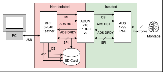
An important topic I mentioned in my introduction to the project is isolation, ensuring there is no conductive path for current through the patient. The architecture is therefore split into non-isolated and isolated domains.
The KiCad schematic captures all this in full detail, which is critical for the EE's. However, for us non-EE types, all those excess squiggly lines just get in the way of understanding (although if you would like to understand pull-up/down resistors, filter chokes, coupling capacitors, etc., see Review: Make: Electronics and Make:More Electronics).
I like to back up to a higher level and draw more abstracted diagrams of the hardware that simplify the view. This is both a learning tool for myself, and a communication tool for others, to convey the architecture so they can grasp it quickly. Then they can dive down into the schematics and datasheets when they need to.
Some people object to drawing such diagrams, because the underlying design may change, obsoleting the diagrams. I often hear the same argument about diagrams and documentation for software. While this is true, keep in mind that this captures a snapshot in time of a particular version of the schematics. They may change, and the diagrams will need to be updated.
This adds to the project maintenance burden. However, I argue that the communication value exceeds the maintenance cost. The diagrams are abstract enough that most changes required should be minor and easy to do. In many cases, no changes are needed. Automated tools that generate diagrams from source material can be a big help.
Here are my interpretations of the schematic as it stands today, sanity-checked by asking the schematic author a few DSWG questions. These illustrate power and signal distribution (drawn with Draw.io/diagrams.net desktop tool and exported as PNG).
Power distribution:
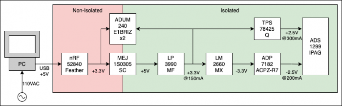
You can see instantly from these diagrams why isolation is needed. The PC connects to 110VAC mains power, and then to the VolksEEG via USB. While dangerous current is not supposed to flow over the USB, isolation is about protecting against unintended flow.
This is part of a common theme in engineering. You always have the happy path and happy day scenarios of a HW or SW design, the way things are supposed to work. But you also have to protect against things going wrong, the unhappy paths and unhappy day scenarios.
There are only a few ways things are supposed to work properly. There are an infinite number of ways things can go wrong. A large amount of engineering effort goes into anticipating and either preventing or mitigating things going wrong. The system must be rendered safe, even when things go wrong.
Anybody and anything can look good when things are going well. It's when there are problems that we see the true test of character, for both people and the systems we build. They have to be robust in the face of problems.
You can also see instantly from these diagrams which chips provide the isolation. Those are the ones bridging the domains. The signal diagram shows why there appear to be duplicated signals on the schematic: there are non-isolated and isolated versions. The ADUM240E1BRIZ-RL chip needs both non-isolated and isolated power, to power it's non-isolated and isolated sides.
This table lists the chips, what they do, and links to their datasheets.
| Part | Function | Datasheet |
| Feather nRF52840 Sense | MCU | PDF |
| MEJ1S0305SC | DC-DC converter, isolation | |
| ADUM240E1BRIZ-RL | Digital isolator | |
| LP3990MF | Linear voltage regulator | |
| LM2660MX | Charge pump switching regulator | |
| TPS78425Q | Linear voltage regulator | |
| ADP7182ACPZ-R7 | Linear voltage regulator negative | |
| ADS1299IPAG | 8-channel AFE |
There's a lot of jargon in all this. Here I'll decode some of it a little.
The ADS1299 is described as an AFE with 8-channel ADC and PGA. That means it's an Analog Front End, with 8 independent Analog-to-Digital Converters and Programmable Gain Amplifiers.
An AFE collects continuous analog signals, in this case from the electrodes arranged in a montage pattern on the patient's head, and the ADC's convert the 8 channels of analog signals to discrete digital data via sampling and quantization. This converts data from the analog to the digital domain that the MCU can use.
The PGA's allow the gain of the signal amplification to be controlled digitally. The input signals are measured in microvolts, which are tiny variations, but the downstream hardware needs to be able to see them in volts to make them usable. The PGA's amplify them to a usable value.
The DC-DC converter and voltage regulators perform DC voltage level boost (increase) and buck (reduction), analogous to a transformer changing AC voltage. A charge pump is a circuit using capacitors to adjust the voltage.


- Comments
- Write a Comment Select to add a comment
All the power is through the feather linear regulator? Just be careful, the implementation does not maximize the rating: per nrf52840-feather/power-management
"We also have the 3V pin which has the output from the 3.3V regulator. We use a 500mA peak regulator. While you can get 500mA from it, you can't do it continuously from 5V as it will overheat the regulator."
To post reply to a comment, click on the 'reply' button attached to each comment. To post a new comment (not a reply to a comment) check out the 'Write a Comment' tab at the top of the comments.
Please login (on the right) if you already have an account on this platform.
Otherwise, please use this form to register (free) an join one of the largest online community for Electrical/Embedded/DSP/FPGA/ML engineers:


