


In this article we’re going to take a look at cycle time, queues, and inventory. Cycle time is a manufacturing term — for anything, not just semiconductors — meaning how long it takes for an individual product to make its way through a manufacturing process, from start to finish. We’re going to try to understand how long it takes to manufacture semiconductors. In particular, we’re going to try to answer these questions:
- How long does it take for a wafer to make its way through the fab? And how long after that to get finished ICs?
- What kinds of steps make up most of the cycle time in a wafer fab?
- What factors influence fab cycle time?
- Is there a tradeoff between cycle time and throughput?
- What strategy do semiconductor fabs use to maximize their throughput, given a limited capital expenditure budget?
In Part Four we went through a recap of how the chip shortage has been doing in 2022, and looked at some dismal predictions of how long it may take for the shortage to end. Certain segments of the semiconductor market, like DRAM and flash memory, microprocessors, and other ICs for consumer electronics, have recovered from supply constraints, and are in a glut due to decreased demand and increases in capacity. Other segments, like industrial and automotive components, still have long lead times and strong demand that seems near-impossible to outpace; their manufacturing processes are the so-called “mature nodes” (40nm - 250nm, more or less) for which foundries have the lion’s share of production but essentially no interest in expanding capacity. It’s a catch-22: the production cost is cheap because the equipment is depreciated, but putting new equipment into use can’t compete with that cost until after it has been depreciated. Adding more mature-node capacity would require enormous capital expense and serious assurance of long-term utilization — and until someone volunteers to cover the cost and risk, the foundries aren’t rushing in to do so themselves. Meanwhile, the automotive market is seeing increasing semiconductor content in each vehicle, with electric vehicles (EV) and advanced driver assistance systems (ADAS) as long-term trends that are fueling demand.
But today we’re going to get back to technical topics, and talk about cycle time.
Cycle time in manufacturing is a necessary but undesirable delay. Semiconductor fab cycle time, in particular is long, measured in weeks or even months. Longer than you might think, longer than it could be, but about as long as it should be. While in the fab, wafers spend the majority of their time waiting in front of machinery. Yes, that’s right, just sitting there, waiting. I’ll explain why this is the case, and why you already know the reasons from everyday life experiences with queues.
I’ll also explain why delays have contributed to the chip shortage, in Part Six, but for now just take it on faith: Delays = Bad. Low Cycle Time = Good. Semiconductor fabs work extremely hard to manage cycle time; this continues to be a hot topic in the field of operations research.
Note that I said manage cycle time, not minimize cycle time. There’s a very easy way to reduce cycle time to near-minimum, but you wouldn’t like it, because it involves lowering the production rate.
For the most part I will be covering the “front-end” manufacturing process — that is, the steps in a semiconductor fab clean room, from blank wafers to finished wafers. There’s also the “back-end” process of taking a wafer, sawing it into individual die, assembling each die into a package, and testing the finished components. I don’t know too much about the back-end steps, but some of the same principles apply.
Disclaimers
Usual disclaimers:
I am not an expert in operations research. I am also not directly involved in the semiconductor manufacturing process. So take my “wisdom” with a grain of salt. I have made reasonable attempts to understand some of the nuances of the semiconductor industry that are relevant to the chip shortage, but I expect that understanding is imperfect. At any rate, I would appreciate any feedback to correct errors in this series of articles.
Though I work for Microchip Technology, Inc. as an application engineer, the views and opinions expressed in this article are my own and are not representative of my employer. Furthermore, although from time to time I do have some exposure to internal financial and operations details of a semiconductor manufacturer, that exposure is minimal and outside my normal job responsibilities, and I have taken great care in this article not to reveal what little proprietary business information I do know. Any specific financial or strategic information I mention about Microchip in these articles is specifically cited from public financial statements or press releases.
Inventory
I want to start with a short tangent about inventory.
One thing that struck me during the worst months of the chip shortage was the inventory reported by different companies. Namely, it wasn’t zero. Or even close to zero.
Many semiconductor companies report days of inventory, either in their quarterly financials or in the earnings calls, and the kind of numbers they were reporting were typically in the 90 - 120 day range. Here are days of inventory for eight of the nine major automotive/industrial semiconductor companies (Analog Devices, Diodes Inc., Infineon, Microchip Technology, NXP, ON Semi, STMicroelectronics, Texas Instruments) over the last three years:

Sure, you can see the dip in 2021 and 2022, but none of them drops below 75 days. That’s two-and-a-half months worth of products! Then why did we have a chip shortage?!
There’s a catch here. We have to define inventory a little more carefully. I talked about automotive inventory in Part Four, with the idea that it was cars and trucks sitting in various places ready to be sold. In semiconductors, perhaps the idea of inventory evokes a picture of warehouses full of chips sitting on shelves. But if you listen to earnings calls, things can get a little blurry, depending on what the speaker is talking about. Here’s Texas Instruments’ Rafael Lizardi during TI’s January 2023 earnings call,[1] in response to a question about how long it will take to balance out inventory:
Yeah, so let me take that. And first, big picture, let me point you to our scorecard, the one that we used for capital management when we talked about the objectives in— when it comes to inventory, is to maintain high levels of customer service, keeping stable lead times while minimizing inventory obsolescence. You know, our strategy and our portfolios is such that it’s long-lived, with a very diverse customer base. So the risk of obsolescence is very low. So that’s a part of the equation.
And the other part is the upside that we get by having that inventory, both short-term and long-term, to support customers. So that’s why we’re comfortable holding higher levels of inventory. I’ve been talking about from current levels, we could add a billion to \$2 billion of additional inventory. And the timing, that all depends on revenue trends. So if they’re higher, then it’ll take longer. If those serving trends are a little weaker, then it’ll be a little faster to get there.
At first glance, Lizardi seems to be painting a picture of chips on shelves to support customers. (Imagine! Two billion dollars worth of inventory, sitting there ready to be sold! Where is this undisclosed warehouse, and how big is it?) But then he says this:
On the mix is a number of angles on that, chip stock versus finished goods, we have a mix of both of those. In some cases, it makes sense to have more of one than the other, but they’re both very low risk. So that’s how we think about it.
What? Chip stock? Huh?
The catch is that a big portion of inventory isn’t chips sitting on a shelf. It’s anything tangible that is expected to be a source of revenue but hasn’t been sold yet. So all those wafers in the fab that haven’t been completed: they still count as inventory.
Renesas was the one major automotive/industrial semiconductor manufacturer that didn’t report days of inventory consistently in a numeric form that I could add to my graph. But I did find a recent presentation from Renesas that points out the different components of inventory, from an accounting perspective:
- Raw materials
- Work-in-process (WIP)
- Finished goods

In general terms, products that are in a partially-complete stage in a manufacturing line are known as work in process or WIP; they start as raw materials, and when they are completed, they are known as finished goods.
The graph on the right shows very clearly that the majority component of inventory at Renesas has been WIP.
In reality it’s a little more complicated. At a high level, semiconductor manufacturing looks like the diagram below. Processes are rectangles and inventory locations are circles.

- Raw materials including blank wafers go into a fab to produce finished wafers
- Finished wafers go through wafer probe (usually in the fab) for each die to be tested with special probes that make contact to pads on the die. Each wafer has an ID, typically scribed on the wafer margin, and the results of testing each die go into a database to form a “wafer map” that keeps track of which die have passed probe and which have failed. In the old days, the method of keeping track was decidedly more low-tech: the die that failed test were marked with a dot of ink.
- Wafers that have been probed go into a die bank. This is a storage facility which may be in the fab itself, or in the assembly facility, or in an external third-party location.
- To produce finished goods (packaged ICs ready to be sold), the wafer is singulated into individual die, which are assembled into a packaged IC and tested. (Failed die that are identified in the wafer map are discarded prior to assembly.)
- Wafer fab and probe comprise the front-end part of the manufacturing process; assembly and test comprise the back-end.
- In some cases, wafers are stored in a wafer bank part-way through the wafer fab process.
What are wafer bank and die bank for? Pericom Semiconductor’s 2013 Annual Report put it this way:
We closely integrate our manufacturing strategy with our focus on customer needs. Central to this strategy is our ability to support high-volume shipment requirements at low cost. We design products so that we may manufacture many different ICs from a single partially processed wafer. Accordingly we keep inventory in the form of wafer bank, from which wafers can be completed to produce a variety of specific ICs in as little as five weeks. This approach has enabled us to reduce our overall work-in-process inventory while providing increased availability to produce a variety of finished products. In addition we keep some inventory in the form of die bank, which can become finished product in three weeks or less.
Die bank is more common than wafer bank, but the idea is the same: one design produces multiple finished goods, and the partially-completed wafer or fully-completed wafer can be stored at the point in the manufacturing process right before that single design diverges into multiple variations. For wafer bank, this would probably be done before the last metal layer or layers, allowing some flexibility in the final manufactured wafer while minimizing time to completion. For die bank, the variation is accomplished during the assembly and test steps: different packaging options can be used, or silicon fuses can be programmed. This simplifies the manufacturing process by deferring the need to specify exactly which product will be manufactured until right before it is sold, so that manufacturers can avoid keeping excess inventory in finished goods. Imagine that one microcontroller has 20 different variant part numbers. (This is fairly common: the one-time costs of product design and manufacturing are so high that multiple variants are usually envisioned to support different package options, temperature ranges, or even memory sizes with a single IC design and mask set.) Without die bank, if the demand for each variant is uncertain, the manufacturer might need to produce excess of some variants to ensure there is stock available. If an order for a million pieces of variant 14 is canceled, and someone needs variant 5 instead, there is no way to convert packaged parts from one variant to another. On the other hand, if a cancellation occurs before assembly and test, then the inventory in die bank can be repurposed for a different customer order.
Die bank is also much closer to the end product, and holding inventory in die bank is much quicker to deliver finished goods than starting from the beginning of the manufacturing process.
There’s also two very tangible cost advantages of holding inventory in die bank.
One cost savings is that the packaging costs don’t need to be spent until a wafer is processed in back-end. The other is the carrying cost of maintaining inventory: imagine a full 200mm wafer of LM358 op-amps. The bare die is only about one square millimeter. The full wafer is about 31000 square millimeters; even with only 67% yield including area lost in the scribe lines, that wafer would yield about 21000 good die. If these were to be assembled as SO-8 parts, the volume of each part is much higher; those 21000 parts would end up in seven reels of 3000 parts each… and the same wafers would need to be split up among different packaging types and temperature ratings, all organized and tracked. Or the wafer could simply be stored in die bank, in a more compact form, all ready to go when needed.
The CFO of Analog Devices put it this way in an August 2022 earnings call:
Die bank is an extremely cost-efficient place for us to hold inventory, particularly when you have 75,000 SKUs. You can hold it— sort of think of it as ten cents on the dollar. So it is very economically efficient and allows us to improve customer satisfaction later on.
Here’s a chart from NXP’s Corporate Business Continuity Update showing some of these different stages of inventory, including die bank:

Inventory is strategically allocated at different points in the manufacturing cycle to help buffer against transient mismatches in supply and demand. For long-lived industrial/automotive products, die bank is where much of the inventory should reside, like water in a primary reservoir. (Short-lived consumer ICs or DRAM that may only have a few years’ potential market is a different story, and holding on to excess content is risky.) Semiconductor manufacturers generally do break down inventory into raw materials / WIP / finished goods, but don’t disclose how much WIP is in die bank or in the front-end or back-end section of the manufacturing line.
Although having extra inventory is helpful when there are surges in demand, there are some major downsides of having too much inventory:
- If it’s not used before it goes obsolete, those parts get scrapped and realize no revenue for the company
- Cost is incurred to organize, maintain, and secure inventory
- The cost of the excess inventory itself could have been deployed elsewhere. A company maintaining \$600M worth of inventory instead of \$500M worth of inventory is using \$100M of funds that could be going into research and development, or sales and marketing, or capital expenses.
Determining the right level of inventory and the right level of production in the presence of all these issues is a huge challenge. It gets worse when we look at the larger supply chain rather than just within a given semiconductor manufacturer, and we’ll see this next time in Part Six.
But I want to come back to the topic of cycle time. Look closely at that NXP chart, showing that time in the fab takes up the majority of the manufacturing cycle, 14 weeks out of 21 in this illustration.
14 weeks?!?!?!!!
Reality Check
Before reading this article, did you have any idea how long it takes to make a finished wafer?
Until a couple of years ago, I didn’t — and I’ve been working in the semiconductor industry for 11 years now! I’m not sure what kind of timescale I had in mind then, maybe a few days?
In February 2022, I put up a highly unscientific poll on Reddit’s /r/ECE (Electrical and Computer Engineering) with these responses:
| Time | Votes |
|---|---|
| 1 day | 18 |
| 3 days | 35 |
| 9 days | 56 |
| 1 month | 63 |
| 3 months | 61 |
| 9 months | 54 |
Quite the spread in answers. So apparently there’s a very unclear perception of how long fabs take to make chips.
The real answer is that it depends, but 1-5 months is probably a good wide-ranging guideline, with simpler processes (analog/power) taking less time, and advanced processes (sub-28nm leading edge) generally taking more time. Here’s what the Semiconductor Industry Association said in February 2021:[2]
Unfortunately, increasing semiconductor capacity utilization takes time, because semiconductors are incredibly complex to produce. Making a chip is one of the most, if not the most, capital- and R&D-intensive manufacturing process on earth. The fabrication is intricate and requires highly specialized inputs and equipment to achieve the needed precision at miniature scale. There can be up to 1,400 process steps (depending on the complexity of the process) in the overall manufacturing of just the semiconductor wafers alone. And each process step typically involves the use of a variety of highly sophisticated tools and machines. In short, making semiconductors is exceedingly hard and, therefore, takes time.
How much time? Manufacturing a finished chip for a customer can take up to 26 weeks. Here’s why: manufacturing a finished semiconductor wafer, known as the cycle time, takes about 12 weeks on average but can take up to 14-20 weeks for advanced processes. To perfect the fabrication process of a chip to ramp-up production yields and volumes takes even much more time — around 24 weeks.
Then, once the fabrication process is complete, the semiconductors on the silicon wafer need to go through yet another stage of production known as back-end assembly, test, and package (ATP), before the chips are final and ready for delivery to the end customer. ATP can take an additional 6 weeks to complete. Therefore, the lead time, which is from when a customer places an order to receiving the final product, can take up to a total of 26 weeks.
This probably skews the answer towards more advanced processes, though. (And it makes a very important error, which has been very apparent in the last two years: this article cites 26 weeks of manufacturing from a blank wafer to a finished chip, but that is the cycle time, not the lead time. Lead time is, as stated, the time from when a customer places an order to receiving a final product, but it can be very different from the cycle time. More on that in Part Six.)
A better answer states the cycle time as a function of the number of photomask layers, typically 1-2 days per mask layer (DPML). Semiconductor Engineering interviewed Robert Leachman of UC Berkeley in 2017:[3]
Generally, the most common metric for cycle time in the fab is “days per mask layer.” On average, a fab takes 1 to 1.5 days to process a layer. The best fabs are down to 0.8 days, Leachman said.
A 28nm device has 40 to 50 mask layers. In comparison, a 14nm/10nm device has 60 layers, with 7nm expected to jump to 80 to 85. 5nm could have 100 layers. So, using today’s lithographic techniques, the cycle times are increasing from roughly 40 days at 28nm, to 60 days at 14nm/10nm, to 80 to 85 days at 7nm. 5nm may extend to 100 days using today’s techniques, without extreme ultraviolet (EUV) lithography.
Estimates of DPML vary slightly. Leachman’s estimate of 1 to 1.5 days per layer seems slightly optimistic; UC Berkeley’s Competitive Semiconductor Manufacturing (CSM) Program reported a performance benchmark of 1.4 days cycle time per layer at full volume[4] in 2000. CSM’s 2002 report on benchmarking eight-inch sub-350nm fabs reported 1.4 to 2.8 days per layer for five industry fabs during 1999 and 2000, with a general downward trend over the 1995-2000 range.[5] Dr. Alvin Loke (now at NXP, then at Qualcomm) stated 1.5 - 2 days per layer in a 2019 presentation.[6] GlobalFoundries’ CTO mentioned 1.5 days of cycle time per mask layer in January 2017.[7] A paper by some engineers at SilTerra Malaysia in 2016 stated:[8]
In 2000, ITRS published the cycle time roadmap for semiconductor fabrication in Factory Integration section for 200mm wafers. The target given for normal production lot was 1.8 DPML for 180 nanometer (nm) technology node. Thereafter, ITRS guidelines no longer publish 200mm technology node roadmap. ITRS shifted focus to 300mm wafers instead and newer technology at 130nm and beyond for new cycle time target. 1.5 DPML was reported in the ITRS 2011 update. 1.3 DPML was reported in Integrated Circuit Economics 2010 Edition as the best cycle time for normal product for 300mm and 2.5 DPML as average.
In year 2010, actual survey claimed by IC Knowledge shows 300mm wafer fabrication performance is at 2.5 DPML.
This number varies by fab, and changes over time within each fab dependent on numerous criteria — but let’s stick with the 1-2 days per mask layer range, with the upper range being more likely.
The reason for using DPML as a metric is that IC manufacturing is very repetitive, going through very similar steps over and over again for each layer. I covered the basic fab process a bit in Part Two; each mask requires essentially the same steps, with minor variations, not necessarily in the order listed below:[9][10]
- cleaning and polishing the wafer
- deposition / ion implantation / diffusion — applying something onto the surface of the wafer to affect electrical properties: metals, silicon, oxides, or dopants. This may involve heating up the wafer in a furnace or may occur after photoresist is selectively removed — see later steps.
- applying photoresist
- exposure — shining ultraviolet light through the mask onto the wafer, to harden selective areas of the photoresist — often referred to as “lithography”, though strictly speaking, “lithography” or “photolithography” describes the whole process
- etch — removing parts of the top layer
- strip — removal of photoresist
- annealing — the wafer is heated in a furnace to mess around with the chemical structure, allowing crystals to “relax” and lower crystal stress or otherwise undergo some sort of chemical reaction. (One of these days I will be able to state what annealing accomplishes, without having to handwave my way through the conversation.)
- metrology and inspection — making sure that the wafer was modified as intended, within appropriate tolerance limits
The ordering is tricky. You’ll see abstract diagrams, like this one, in various journal articles on semiconductor manufacturing, that make me think of some kind of Kafkaesque game where you are stuck going around in circles trying to get free:

Abstract process flow of typical semiconductor manufacturing, redrawn from Hsieh & Hsieh[11]
It’s not a repeated linear progression through the same steps. This is easier to see if you were to look at a real process flow. The best I can do is to show the steps in one of the CMOS processes mentioned in the MIMAC project test data.[12] This was a SEMATECH study published in 1995, which included datasets taken from manufacturing data in production fabs:
In a separate effort, SEMATECH assembled several factory-level datasets. European data was added and validated under the MIMAC project. The purpose of collecting the datasets was to aid academics and suppliers in developing new models and tools for industry. The datasets contain actual manufacturing data from both ASIC and logic wafer fabrication facilities, organized into a standard format. They include no real product names, company names, or other nomenclature that could serve to identify the source of the data. Each dataset contains the minimum information necessary to model a factory, including product routings and processing times, rework routings, equipment availability, operator availability, and product starts.
Each MIMAC dataset includes a spreadsheet listing the process steps used for each of several sample products. This is not a complete recipe (“Add two cups of gallium phosphide. Heat to 925 °C and stir briskly....”) but it does give a short name for each step, along with a few timing details required to run a factory simulation. For the most part, the names and details are enough to figure out what category of tools are used in each step. In the figure below, I have drawn the process flow for Product 1 in Set 4, a microprocessor of some sort:

Process flow of Product 1 in MIMAC Set 4. Steps numbered in order in circles. White circles represent steps utilizing common tool groups. Green circles represent a cleaning step. Purple circles represent other steps.
Product 1 utilized a very minimal CMOS process with nine mask layers including one metal layer, probably dating back to the late 1980s.[13] Each mask layer goes through the same process of coating photoresist, running through an aligner for the exposure step, developing and baking the photoresist, doing something else, and then going through a resist “strip” process (with piranha solution!) to remove the photoresist. But the other steps of the process vary with each layer. For instance, many of the so-called front-end-of-line (FEOL) steps, which construct the transistors, resistors, and capacitors, require ion implantation. The back-end-of-line (BEOL) steps to interconnect the integrated circuit elements do not use ion implantation: the “APS” layer (aluminum to polysilicon & silicon contact), “Alum” layer (aluminum metal traces), and “Silox” layer (silicon dioxide for passivation) involve mostly thin-film deposition, furnace, and etching steps.
As far as number of layers in typical fab processes, here are some examples to give you a flavor of how this has changed over time:
-
The MOS 6502 required seven masks in 1975: a minimalist approach to NMOS fabrication, with one metal layer. Time through the MOS Technology fab took somewhere between 2 and 8 weeks, working 24 hours a day, 5 days a week.[14]
-
The CMOS process from the MIMAC dataset, as mentioned above, required nine masks, with one metal layer.
-
Today’s leading-edge ICs have multiple metal layers and all sorts of complexity, so that their mask layer count gets up into the dozens. Leachman’s estimate of “a 28nm device has 40 to 50 mask layers” is one data point; another is from a 2016 article quoting a director at Samsung at 40 mask layers for 45nm/40nm:[15]
“We started to see the mask count at about 40 mask layers at 45nm/40nm,” said Kelvin Low, senior director of foundry marketing at Samsung. “That grew into 60 mask layers for the 14nm and 10nm node. If you push that without EUV, and stretch immersion into triple or quadruple patterning, we expect the mask count to go to about 80 to 85 at 7nm. In some cases, you could see 90 mask layers, depending on the area scaling that you are trying to target. We think maybe one or two companies can afford this technology. The masses probably cannot afford this technology.”
-
Intel’s 90nm – 32 nm processes saw a gradual increase in metal layer count:[16]
- 90nm (2003) — 7 metal layers
- 65nm (2005) — 8 metal layers
- 45nm (2007) — 9 metal layers (metal 9 much coarser, for power distribution)
- 32nm (2009) — 9 metal layers (metal 9 much coarser, for power distribution)

Top row: Scanning electron microscope (SEM) cross-section of MOSFET junctions; Middle row: SEM cross-section of interconnect; Bottom row: Die photomicrograph. From Bohr & Mistry, Intel’s Revolutionary 22 nm Transistor Technology[17] (Credit: Intel Corporation)
-
Intel’s 14nm process, used in its Broadwell architecture, included 13 metal layers,[18] the lower 12 of which can be seen in this cross-section:

Scanning electron microscope (SEM) cross-section of Broadwell IC, from Bernasconi and Magagnin,[19] CC BY-4.0.
-
Freescale (now part of NXP) MPC561 microcontroller (2004): 250nm process, 3 aluminum metal layers.[20]
-
Freescale ATMC C90FG process used in the MPC5674F (early 2010s): 90nm, 6 copper metal layers, 55 mask layers, 350 process steps.[20]
-
Infineon C11N process, 130nm CMOS, 4-6 metal layers, circa 2007.[21]
-
SilTerra’s CL110AL process, 110nm, up to 6 metal layers, circa 2013.[22]
-
ST Microelectronics CMOS M10 process, 90nm, 4-6 metal layers.[23]
-
TSMC 45nm: 9 metal layers (7 small-geometry and two large power distribution metal layers)[24]
Metal layer count is important because each metal layer in modern fab processes requires at least two masks: one for vias to other layers and one for the metal itself. (You can see this in the Intel SEM images above, and in the “Metal layer manufacturing” diagram below.) It seems likely that most microcontrollers affected by the chip shortage (40nm – 250nm) would have between 3 and 9 metal layers, which therefore adds between 6 and 18 mask layers to whatever is required by the active and polysilicon layers (the FEOL steps) and a passivation layer at the end.
Metal layer manufacturing, from International SEMATECH 1999 Annual Report.
Smaller geometry processes (22nm FinFET and under, and maybe 28nm) start to require multiple patterning steps, which requires more masks and more process steps, and therefore increases cycle time — thankfully something that didn’t impact the “mature nodes”.
There are hundreds of steps (called “moves”) in a modern semiconductor fab. In addition to the sheer number of steps, there are some nuances that differentiate the kinds of processes that go on in a fab. Here’s an overview that I think helps give some flavor of those nuances:[25]
The semiconductor manufacturing process is performed in a clean environment known as a wafer fabrication facility or wafer fab. The steps required to manufacture a semiconductor product or device are described in a process flow or process routing; current generation semiconductor process flows can contain between 250 and 500 manufacturing or processing steps. Typically, the individual silicon wafers upon which semiconductors are manufactured are grouped into “lots” of 25 wafers. Each lot is uniquely identified in the wafer fab’s manufacturing execution system (MES) as a unit of production (job). Therefore, the individual wafers within a lot travel together throughout the manufacturing process.
The equipment set used to manufacture semiconductors is typically made up of 60 to 80 different equipment types. These equipment types contain a diverse array of wafer processing tools in terms of the quantity of wafers that can be processed concurrently. While single wafer tools (photolithography steppers) only process one wafer at a time, other tools (acid bath wet sinks) can process entire lots concurrently. Wafer fabs also contain batching tools (diffusion furnaces) that can process multiple lots of wafers simultaneously. Finally, some tools (ion implanters) are subject to sequence-dependent setup times, as the time required to setup the tool depends upon the previous lot that was processed on the tool.
Due to the production volumes required in today’s wafer fabs, these fabs contain multiple tools of each equipment type. This redundancy leads to the notion of a workstation or “tool group” made up of similar tools of a given equipment type that process wafers in parallel. Finally, semiconductor process flows contain a considerable amount of reentrant or recirculating flow, wherein a given tool may be visited a number of times during the manufacturing process by the same lot (job). This type of flow is necessitated by the capital cost of wafer processing equipment, which can cost up to \$7,000,000 per tool.
So: hundreds of steps, some are batch tools, some tools operate on single wafers, and they’re very expensive.
If you were paying close attention in Part Two, MOS Technology’s “019” process took 50 steps to complete the seven mask layers used in the 6502. Even that is a lot to take in, so to understand the general behavior of a fab, we’re going to take a detour from semiconductor manufacturing and look at a few simpler examples.
Freddy’s Forgery Factory
Freddy Flannery’s from Fresno.
Freddy found fame and fortune from art forgery. Freddy’s forté: forgotten works, famous Frenchmen. Cézanne, Degas, Gauguin, Renoir, Matisse, Monet… and finally—
Felony.
Five years, Folsom.
Freddy, freed but fatigued, found legitimacy in mass production. Freddy’s plan: a factory in Fresno, churning out first class facsimiles of famous works, framed.

The manufacturing process that Freddy had in mind — just imagine this running through Freddy’s head as he is falling asleep on his prison bunk — consisted of a few different machines connected by conveyor belts, roughly equivalent to the ones shown below:
Each machine loads canvases until it is full — one canvas for the single unit machines, several canvases for the batch machines — and then processes the canvases. When processing is done, it begins unloading; if there is no space on the unloading conveyor, the machine has to wait. (Continuous-process machines like the conveyor ovens don’t have a loading/unloading process, only a transport delay.)
For our purposes, the exact operations of these machines don’t matter; we just care about the timing of the products (canvases) as they travel along the manufacturing line. (Note: I am also not an art forger, so presumably machines like the ones illustrated here are unrealistic.) One major goal of manufacturing is to make sure there aren’t problems by keeping track of how the WIP is moving through the factory.
Here’s the whole factory shown in a more compact layout:
Freddy planned this very carefully, so he could manage both the throughput and latency of this process. The raw process time per painting is the sum of all these times, or 82 minutes. In Freddy’s factory, each machine (except for the conveyor oven) also takes a total of 30 seconds to load or unload each canvas, and the conveyor belts add a transport delay of 60 seconds for each step, when they are moving at full speed. By Freddy’s calculations, this adds another 12 minutes, for a total latency or cycle time through the factory of 94 minutes.
The throughput is dependent on the maximum rate of each step. In Freddy’s factory there are six equal bottlenecks of 5 minutes per painting:
- the two aging ovens take 18 minutes to process and 2 minutes to load/unload a batch of four paintings, for a total of 20 minutes = 5 minutes per painting
- the inkjet and brush machinery and the two inspection stations take 4.5 minutes to process + 30 seconds to load/unload = 5 minutes per painting
At 5 minutes per painting, that’s 12 paintings per hour. Freddy’s factory was designed to operate 24/7, so it should be capable of producing 288 paintings per day. Freddy fell asleep numerous times with visions of millions of dollars rolling in.
At least that’s what Freddy figured. The reality was a little different; Freddy made some serious mistakes in his calculations because he forgot to take into account some important limitations of manufacturing, namely yield loss, variability, queueing delays, and maintenance.
The on-line visualizations of Freddy’s factory don’t include yield loss — we won’t cover yield loss here; imagine that a defect is found during inspection, and the canvas can either be reworked or scrapped, with a decrease in production rate either way. But the other factors are there. If you wait a while, the storage pile at the end will show the cycle time of the most recently completed canvas:

123 minutes and 30 seconds?! That’s almost a half hour longer than Freddy’s 94 minute calculation. Where did the extra cycle time come from? (Hint: try reducing the “Canvas starts” slider to 8/hour, and look at cycle time as well as the flow of canvases through the factory. If you’re impatient, increase the simulation speed. I’ll reveal the answer later in the article.)
At any rate, let’s assume for the moment that 288 paintings per day is the factory capacity. The most serious error, perhaps, is that Freddy assumed demand was high enough to sell those 288 paintings per day. Over the long run, Freddy can’t produce more than he can sell, or he’ll end up with a growing number of unsold paintings in inventory, so he will likely be running at some lower rate, perhaps 144 paintings per day. The ratio of the actual production rate to factory capacity is the utilization of the factory: 144 paintings per day / 288 paintings per day = 50% utilization.
The cycle time of Freddy’s factory will change depend on the utilization; with everything else fixed, the cycle time is some function of utilization, called the operating curve. Operating curves look something like this:
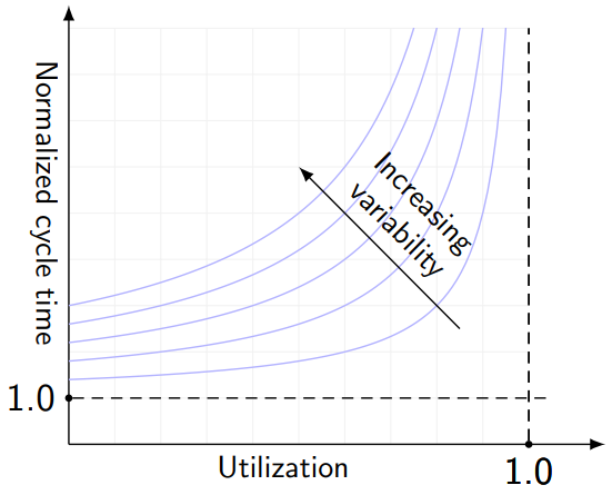
This graph shows normalized cycle time, which is cycle time divided by its theoretical minimum, so that can never drop below 1. As the factory approaches 100% utilization, the cycle time zooms upwards, with a scaling factor that depends on variability in the factory.
Let’s look at another factory, and then I’ll talk about why these curves are the way they are.
Supply Chain Games 2022: Shapez
If you want a virtual factory experience that’s a little more engaging than Freddy’s Forgery Factory, I would suggest trying out Shapez, an in-browser game that has factory elements. (I’ve been told that I should try out Factorio, but from what I can tell it has an excess of evil addictive complexity, so I’ve avoided it so far.)
In Shapez, you are in a large grid with various deposits of shapes and colors. You start out next to a big squarish thing called The Hub, which demands you produce and deliver it various quantities of shapes.

To do this, you place Extractor machines onto one of the grid squares in a shape or color deposit, and it starts extracting the shape or color at a regular rate, initially 1 item every 2.5 seconds = 0.4 items/s. You can place conveyor belts to bring the extracted shapes to the Hub. There are other machines as well — cutting machines, rotators, balancers, stackers, painters, tunnels, etc. — which process the shapes as demanded by The Hub.
The game starts simple, but each time you produce enough of the target shape, it gets more complicated, and new machines are unlocked.
One of the challenges of the game is that not all the machines process at the same rate. If a machine doesn’t have one of the inputs it needs, the machine will wait. If an input arrives faster than it can process, the raw material will back up on the conveyor belts leading into the machine, and the belts leading out of the machine will have lots of empty space. These are signs of a local bottleneck: upstream inputs backing up, downstream output with empty space. In the image below, the cutting machines appear to be a bottleneck. (They are, for the most part. Taking a closer look, I see I haven’t divided up the semicircles equally among the painting machines. The lower conveyor belt runs through a balancer that splits up the content and diverts half of the semicircles onto a belt destined for the painting machine on the left, which gets the majority of of the semicircles, so the input belt that leads from the top cutter is backed up, waiting to sending semicircles through the tunnel and on into the painting machine. But the conveyor downstream from the painting machine is backed up also.)

One of the ways that you can compensate for unequal processing rates is to build repeated sections of machinery that each draw off part of the material from the conveyor belts, processing it in parallel with other sections. Here’s an example, showing three stackers that each grab a red circle from one conveyor belt and a green circle from another conveyor belt, stack them together, and put the resulting watermelon sections out through a tunnel onto a third belt.

At some point I realized there was extra space (note that only three out of every four grid rows are doing something), so I rebuilt it as part of a much larger ladder — with 12 stackers in parallel! — in a section of machinery constructed to deliver a 90-degree slice of watermelon to The Hub. In the big picture, the bottleneck is in a different area, containing cutting machines.
The bottleneck depends on the different processing rates — which, by the way, you can speed up by collecting enough shapes to upgrade your machinery.

Improving throughput in Shapez is all about finding bottlenecks, and adding more machinery to relieve those bottlenecks. Visual identification is usually pretty easy, but sometimes it helps to analyze numerically. Below is a snapshot of one section of machinery with three painter machines in parallel at 0.33/s, for an aggregate capacity of 0.99/s, and two cutter machines in parallel at 0.75/s each, for an aggregate capacity of 1.5/s. At the time I was playing, the conveyors and tunnels could handle 3 shapes per second.

So I could triple the number of painter machines and double the number of cutter machines to reach that 3 shapes per second throughput:

It’s easy to see when you get to this point: the conveyor belts are all full of work in process, with no space in between.
I had to fix a couple of things, though, that I had missed on first glance:
- the extractors are limited to 0.8/s, so I need four of them at the blue and square deposits to keep up with the demand of 3 shapes per second
- cutters output twice as many shapes as their input, so that produces 6 shapes per second, which I need two conveyor belts to carry.
But I did it! Now the bottlenecks are the conveyors and painters and cutters, all operating with a net throughput of 3 shapes per second in, 6 blue rectangles per second out. Like we saw in Supply Chain Idle in Part Three, the optimum factory design is when we balance the production capacity until we get 100% utilization on as many machines as possible.
Or is it?
The Missing Ingredient is Variability
That’s a trick question, because both Supply Chain Idle and Shapez are not like the real world. Both games — as well as Freddy’s ideal vision of a factory — are perfectly happy to run like clockwork. Chances are, if you’ve seen any video footage of a factory, it’s a smooth, hypnotic, fast-paced flow of stuff, like this beer bottling plant:
Look at that, zoom zoom zoom, everything is perfect, poetry in motion.
Some factories are like the beer bottling plant. But some are not, and the difference is all in how material flows through the factory. Smooth flows of material through the factory are known as synchronous. Imagine for a moment that there are 240,000 people drinking beer in some region of the world, and each of them drinks two bottles a day. The local beer bottling plant produces 480,000 bottles per day, packing them 24 to a case, 20,000 cases a day, sent to nearby stores and restaurants. Everything is balanced, with all the steps in the bottling plant running at the same rate, producing exactly enough to match the demand of one bottle every 0.18 seconds — this is known as the takt time — and everyone is happy.
James Ignizio puts it this way:[26]
The basis for the belief that a factory should employ a balanced line running at takt speed is a consequence of a narrow focus on synchronous factories. An ultimate example of a synchronous factory might be that of a soft-drink bottling plant. In such a plant, the flow of each job (i.e., each bottle) is synchronized with every other job. There is no extra room on the conveyor belt connecting one workstation to another, so balance and synchronization are essential.
Automobile assembly lines, while not necessarily strictly synchronous, are very close to being synchronized. In a moving automobile assembly line or a perfectly synchronized line, a balanced line makes sense. But this does not hold for asynchronous factories such as semiconductor wafer fabrication facilities.
What may not be obvious is how difficult it is to achieve synchronous flows in a manufacturing plant, or the disadvantages of trying to run synchronous flows, or what happens when flows are not synchronous, or why some manufacturing processes are naturally synchronous and some are not.
(There’s some really deep thoughts lurking here, by the way. I think I understand the situation enough to provide an explanation for some of those topics, but realize that there have been major differences of opinion even among manufacturing professionals about the optimal way to run different types of factories, so don’t treat what I have to say as the gospel truth.)
The key feature of an ideal synchronous manufacturing plant is that the cycle time is purely dependent on processing steps and the transport time to get through the plant. There is never any wasted time: the beer bottles in the plant are not waiting for machinery, and the machinery is never waiting for beer bottles. Either of those cases represents lost opportunity. If the machines wait for more products to arrive, then they aren’t fully utilized. If the products are waiting for machines, then cycle time is longer than necessary, and the factory needs space for those products to wait.
In a sense, the synchronous manufacturing plant represents perfection, and any deviation from that synchronous flow reduces the plant’s ability to keep cycle time to its theoretical minimum.
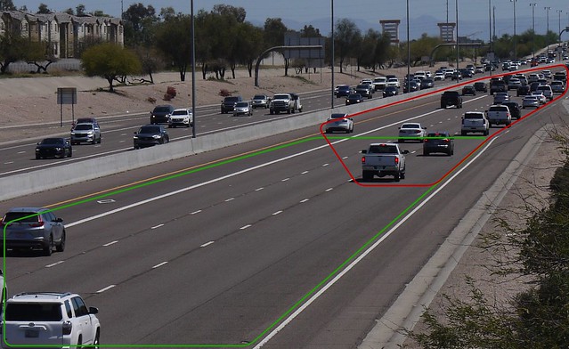
There are common real-world situations that have some similarity to the challenges of the synchronous flow in a factory; one of them is highway traffic. In heavy traffic, smooth vehicle flow is impaired, and both of the following tend to happen:
- Traffic density is high enough that vehicles are forced to slow down and wait to proceed
- Traffic density is lower in other places, and represents a lost opportunity; if only the flow of traffic were more uniform, then there would be fewer slowdowns.
The first of these is familiar to us, as a traffic jam; the second may not be. Both are visible in this picture:
One alternative to irregular vehicle flow in highway traffic should also be familiar to us: consider a freight train, with each car connected to the next, all traveling synchronously together. The freedom of each car on a highway to travel at its own speed — as long as it doesn’t run into the vehicle in front — allows variability, and we get traffic jams when there are enough cars on the road.
Keep that thought in the back of your mind. We’re going to look at another example to understand the effect of variability in a factory a little more clearly. Variability can put us in dire straits. Which reminds me, we need some music.
Notes
[1] Seeking Alpha’s transcript of TI’s earnings call for Q4 2022 misattributes this response to Dave Pahl. [2] Semiconductor Industry Association, Chipmakers Are Ramping Up Production to Address Semiconductor Shortage. Here’s Why that Takes Time, Feb 26 2021. [3] Mark LaPedus, Battling Fab Cycle Times, Semiconductor Engineering, Feb 16 2017. [4] Robert C. Leachman and David A. Hodges, Competitive Semiconductor Manufacturing: Program Update, University of California at Berkeley, Jul 8 2000. [5] Robert C. Leachman, Competitive Semiconductor Manufacturing: Final Report on Findings from Benchmarking Eight-inch, sub-350nm Wafer Fabrication Lines (CSM-52), University of California at Berkeley, Mar 31 2002. The cycle time per layer measurements are graphed on page 49. This report covers ten industry fabs, anonymized as “M1” through “M10”, but included reported data in the 1999 and 2000 range from only five of them. An earlier report, CSM-31, published in 1996, covered a wider range of fabs (including AMD, Cypress, Intel, IBM, Lucent, Motorola, National Semiconductor, Samsung, TSMC, Texas Instruments, Toshiba, and UMC) measured over the 1992–1995 timeframe. This report included cycle time data from CMOS logic fabs (1.8 – 3.3 days per layer) and Medium Scale Integration fabs (analog circuits and power devices; 1.2 – 3.7 days per layer). [6] Alvin Loke, IEEE CICC2019 ES2-2: Nanoscale CMOS Implications on Analog/Mixed-Signal Design, IEEE Custom Integrated Circuits Conference, Apr 2019, posted on YouTube Dec 18 2019. Unfortunately the video was removed, and I can’t find any written records with the 1.5 - 2 DPML mentioned. Slides are still available; Dr. Loke mentioned cycle times on slide 40. [7] David Lammers, Innovations at 7nm to Keep Moore’s Law alive, Solid State Technology, Jan/Feb 2017. The article cites a statement by GlobalFoundries’ CTO Gary Patton, speaking at the SEMI Industry Strategy Symposium in January 2017. [8] Kader Ibrahim, Mohd Azizi, and Uda Hashim, Semiconductor Fabrication Strategy for Cycle Time and Capacity Optimization: Past and Present, Proceedings — International Conference on Industrial Engineering and Operations Management, Mar 8-10, 2016. [9] Jessica Timings, Six Crucial Steps in Semiconductor Manufacturing, ASML, Oct 6 2021. [10] Microcontroller Division Applications, AN900: Introduction to Semiconductor Technology, STMicroelectronics, 2000. [11] Liam Y. Hsieh and Tsung-Ju Hsieh, A Throughput Management System for Semiconductor Wafer Fabrication Facilities: Design, Systems and Implementation, Processes, Feb 11 2018. Article published under a Creative Commons Attribution (CC BY) license. [12] John Fowler and Jennifer Robinson, Measurement and Improvement of Manufacturing Capacity (MIMAC)
Designed Experiment Report, Jul 20 1995. Datasets available online at FernUniversität in Hagen website. [13] NMOS microprocessors dominated until the mid-1980s; CMOS microprocessors of this era were the Western Design Center 65C02 (1983), Intel 80C51 (1983), Motorola 68HC11 (1984), Motorola 68000 (1985), and Intel 80386 (1985). The single metal layer of MIMAC Microprocessor Product 1, and the fact that it was still in production in the early 1990s may imply some kind of low-cost long-lifetime microcontrolller. (Intel’s CHMOS-III process used in the 80386 was a 1.5-micron process with two metal layers, according to the company’s “Introduction to the 80386” databook.) [14] I got a couple of different answers from various staff members at the MOS Technology plant in Pennsylvania during the NMOS days (1970s - early 1980s). Bil Herd, designer of the Commodore 128, who worked at MOS from 1982 – 1986 remembered “about a month for a full run”. (pers. comm. Mar 16 2022) Herd spoke at Vintage Computer Festival Midwest 11 in September 2016, recounting that “it’d take another quarter million dollars and three or four weeks to spin the chip to do another rev of it.” Bill Barnhill, who worked in the fab on equipment maintenance and process development from 1973 – 1986, remembered “a standard batch of wafers took between two to three weeks to go through the fabrication area. Special runs could be made in 10-14 days but that was mainly for new improvements or changes to the process.” (pers. comm. Jul 15 2023) MOS/Commodore ran the fab 24 hours a day, 5 days a week, with maintenance “performed on the weekend to eliminate downtime”. (pers comm. May 18 2022) Albert Charpentier, lead designer of the Commodore 64 chipset, who worked at MOS from 1975 – 1982, remembered 6-8 weeks as the standard fab manufacturing turn time, with 2-3 weeks under expedited circumstances. According to Charpentier, the Commodore/MOS fab “turned the VIC-II R1 in about a little more than a week to make January 1982 CES.” (pers. comm. Jul 16 2023) A one-week turnaround through wafer fab is unheard of these days, due to process complexity; even then, with a 7-layer NMOS process, and downtime on weekends, this would have been less than a day per mask layer. A 1985 IEEE Spectrum article (Tekla S. Perry and Paul Wallich, Creating the Commodore 64: The Engineers’ Story, Mar 1 1985) states: David A. Ziembicki, then a production engineer at Commodore, recalls that typical fabrication times were a few weeks and that in an emergency the captive fabrication facility could turn designs around in as little as four days. There would likely have been some variation in cycle time as the business cycle progressed and led to fluctuations in MOS/Commodore’s fab utilization. [15] Mark LaPedus, Mask Maker Worries Grow, Semiconductor Engineering, Aug 18 2016. [16] Intel IEDM papers for the 90 – 32 nanometer range: [17] Mark Bohr and Kaizad Mistry, Intel’s Revolutionary 22 nm Transistor Technology, Intel Newsroom slide presentation, May 2011. [18] Sanjay Natarajan et al., A 14nm Logic Technology Featuring 2nd-Generation FinFET , Air-GappedInterconnects, Self-Aligned Double Patterning and a 0.0588 m2 SRAM cell size, 2014. Intel publishes details on its processes in papers submitted to the IEDM, and usually includes dimensions of the metal layers, but didn’t put much detail for the 14nm process. [19] Roberto Bernasconi and Luca Magagnin, Review—Ruthenium as Diffusion Barrier Layer in Electronic Interconnects: Current Literature with a Focus on Electrochemical Deposition Methods, Journal of The Electrochemical Society, Dec 10 2018. [20] John Cotner, Semiconductor 101: Functionality and Manufacturing of Integrated Circuits, Freescale Semiconductor, Sep 2013. What a great set of slides! Includes several dozen just on wafer fab processes. [21] Infineon, C11N 130nm CMOS Platform Technology, publication date Sep 2007. [22] SilTerra website, https://www.silterra.com/technology/. See also SilTerra slide deck, Ibero-America IC Design Contest, Apr 25 2013, slide 22: CL110AL listed as available Q1/Q2 of 2013. [23] STMicroelectronics, Product Change Notification PCN APG-MID/13/8204, Nov 5 2013. [24] Kuan-Lun Cheng et al., A highly scaled, high performance 45 nm bulk logic CMOS technology with 0.242 μm2 SRAM cell, 2007 IEEE International Electron Devices Meeting, Dec 2007. (“7+2M BEOL process” shown in Fig 12.) [25] Scott J. Mason and John W. Fowler, Maximizing Delivery Performance in Semiconductor Wafer Fabrication Facilities, Proceedings of the 2000 Winter Simulation Conference. [26] James P. Ignizio, Optimizing Factory Performance, 2009.
Sad Fish Bank
We’re going to take a look at a very simple queuing example: La Banque du Poisson Maussade, a hypothetical bank located somewhere in Europe, quite possibly in Belgium. This bank is very efficient. It is open 24 hours a day, 7 days a week, with no holidays. It has one entrance door, one exit door, and one teller, who can process requests instantly. Oh, and there is space inside the bank for about 50 people to wait in line, with a much larger secondary waiting area, which may make you suspicious that there is a catch.
There are three catches, actually:
- The bank only handles deposits and withdrawals.
- Yes, the teller processes requests instantly, but at random.
- As long as there is room, the entrance door lets people in at random.
At random? What does that mean, exactly? And why does it matter?
Random Processes: Radioactive Decay and Telephone Calls
Any one who considers arithmetical methods of producing random digits is, of course, in a state of sin.
— John von Neumann, Symposium on the Monte Carlo Method, 1949
The entrance doors and teller are examples of random processes, meaning something that happens unpredictably. But many random processes can be characterized statistically. In this bank, the entrance and teller are each modeled by an average rate of events.
(Warning! This section contains mathematics! I’ll try to keep it brief and simple. If you get overloaded by the math, either take a deep breath and ignore it while you keep reading, or just skip ahead until you see the section Math takeaways.)
For example, the arrival rate \( \lambda \) (lambda) characterizes entrance events: in any given small interval of time \( \Delta t \), the probability that someone walks in the entrance is \( \lambda \Delta t \). If \( \lambda = 0.01/s \), then during each second, there is a one-in-a-hundred chance that someone will walk through the door; during each millisecond, there is a one-in-a-hundred-thousand chance that someone will walk through the door. There is always the possibility that as you turn and look at the door, one person walks through the door during the first millisecond and another person walks through the door less than a millisecond after the first. This would happen infrequently (about one in ten billion each millisecond, according to this model, which would happen on average about once every four months) and is not very realistic — in real life, it would take a couple of seconds for one person to pass through a doorway and allow the next person to enter. But in our model, that doesn’t occur: each entry event is instantaneous and independent. The time between entry events, called the interarrival time, has a mean value of \( 1/\lambda \), so with \( \lambda = 0.01/s \), the average time between people entering the bank is 100 seconds. The interarrival times are random, and happen to follow an exponential distribution.
The teller also processes customers at a certain rate \( \mu \), with the same characteristics: within any given small time interval, if there is a customer waiting for the teller, the probability that the teller will finish processing the customer’s request is \( \mu \Delta t \).
This kind of system is called an M/M/1 queue; the M stands for Markovian — all events in both arrival and servicing are independent of past history, also called a Poisson process — and the 1 means there is a single server, sometimes indicated as shown in the diagram below:

The behavior of a queue is the subject of the field of queueing theory, which was first formalized by A. K. Erlang in 1909. Erlang published a paper while working at the Copenhagen Telephone Company to analyze the mathematical properties of telephone traffic. But man-made inventions are not the only things that can be characterized using queueing theory. Events characterized as a Poisson process with some rate \( \lambda \) are fairly common in the real world, in any situation where these events are part of a recurring process and there are no reasons for them to occur at any particular time relative to other events: radioactive decay, rainfall, shot noise in electric currents — in addition to telephone network traffic. These are all good examples of arrival events.
The modeling of a bank teller’s service times by a Poisson process, on the other hand, is kind of odd — but let’s stick with it for now.
The math behind an M/M/1 queue is fairly simple, and we can draw it as a Markov chain with each state denoting the number of customers inside the bank:

The arrows between states show the transition rates: customers arrive at rate \( \lambda \), increasing the state by one each time a customer arrives, and customers depart at rate \( \mu \), decreasing the state by one each time a customer is serviced at the teller.
The interesting part of queue analysis starts to happen when you answer questions about the behavior of the queue. For example, if I walk into the bank as a customer, how long is my expected wait and how many customers are likely to be ahead of me?
The M/M/1 queue has a steady-state probability distribution in each state \( k \) of \( P[k] = (1-\rho)\rho^k \) where \( \rho = \lambda/\mu \) is the utilization of the queue. For example, if \( \lambda = \) 2 customers per minute and \( \mu = \) 3 customers per minute, then \( \rho = \) 2/3, and there’s a 1/3 chance of zero customers in the bank, 2/9 chance of one customer in the bank, 4/27 chance of two customers in the bank, 8/81 chance of three customers in the bank, and so on. The probability that there are at least \( k_0 \) customers in the bank (in other words, \( k \ge k_0 \)) is \( \rho^{k_0} \). This means there might be at least 50 customers waiting in line! The probability of this happening at any given instant is really small; for \( \lambda = 2, \mu = 3 \), this probability would be \( (2/3)^{50} \approx 1.568 \times 10^{-9} \), or a little more than one in a billion. But you can’t rule it out!
So how large should the bank’s waiting area be? That’s much harder to answer. In this example, at first glance, if we want the probability for the queue to overflow to be less than one in a billion, then it seems like room for 50 customers should be adequate: 50 customers fit, 51 do not, and the probability of at least 51 customers is \( (2/3)^{51} \approx 1.046 \times 10^{-9} \). But that’s the probability of this occurring at any given instant that we choose to look at the bank. If we restated that we wanted the probability of the queue overflowing at least once during an entire year of operation to be approximately 1%, it would require a queue capacity of 40. (The probability of overflow in this case is approximately \( 1-e^{-Lt} \) where \( t= \)1 year ≈ 526000 minutes and \( L = \lambda(1-\rho)^2\rho^{40} \approx 2.0097\times 10^{-8} \)/minute, leading to an overflow probability of about 0.0105. Real-world situations would probably just handle the situation by the natural distaste of customers deciding not to enter the bank if the line is too long.)
As for my original questions, with \( \lambda = \) 2 customers per minute and \( \mu = \) 3 customers per minute:
- How long is my expected wait? The expected wait time (time in the bank before I get to the teller) is \( 1/(\mu - \lambda) - 1/\mu = \) 40 seconds, and the expected service time after getting to the teller is \( 1/\mu \) = 20 seconds, for an expected total time of \( 1/(\mu-\lambda) = \) 60 seconds.
- How many customers are likely to be ahead of me? The expected number of customers in line when I arrive is \( \sum\limits_{k=0}^{\infty}kP[k] = \frac{\rho}{1-\rho} \) which is (2/3)/(1/3) = 2.
The derivation of these is probably a good exercise for math students, but too much of a distraction here, so I’ll just refer to Wikipedia.
Why do we care about the random aspect of arrival and service times in queues? The main reason is that it causes temporary mismatches between the entrance and exit rates of the queue. During some periods of time, we will have more items entering than exiting the queue, and the queue length will increase. In other periods of time, the server will process queue items faster, and the queue length will decrease. And when the queue becomes empty, it represents lost opportunity: the server must sit idle, waiting for something to do.
Weird things happen when the utilization \( \rho=\lambda/\mu \) approaches 1 or even exceeds it… but rather than trot out some equations, let’s see our bank in action!
At La Banque du Poisson Maussade, the teller’s service rate is \( \mu = \) 2/minute — an average service time of 30 seconds — and there’s a 2-second “walk-up time” for the customers to step up to the teller, for an effective net service rate of \( \mu’ = 1/(32 \mathrm{s}) = \) 1.875/minute. This gives a utilization of \( \rho = 1.0667 \)… greater than one… yikes! If you crank up the simulation speed, you’ll see the customers pile up, with a brief reprieve at around 7 hours where the customers are lucky enough that the teller catches up — but then after that the pile-up happens again in earnest.
If you want to see the case of \( \rho = 2/3 \), where the expected number of customers in line is 2, you’ll need to change the arrival rate \( \lambda \) down to 1.25/minute.
Over a long time, if \( \rho > 1 \) the pile-up or overflow rate is somewhat consistent; here’s a sample run of the first 96 hours of operation at \( \lambda = 2.0 \):
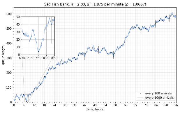
The overflow rate \( \lambda - \mu = \) 0.125/minute = 7.5 customers per hour, so after 96 hours we should expect around 720 customers, with some variability — in this sample run there is just under 600. This variability can be quantized: the standard deviation of queue length \( N(t) \) for \( \rho > 1 \) increases with time, approximately \( \sigma_N = \sqrt{(\lambda+\mu)t}, \) and at very large time scales, the effect of randomness becomes less significant compared to the mean. Over the course of 500 hours the queue length meanders around, staying mostly within one standard deviation of the mean.

If we’re planning a factory or a bank running for a long time, we need to take into account both effects: the mean values will dominate over the long term, but we can’t ignore the short-term random fluctuations or the worst-case behavior will overload our system.
Of course, the \( \rho > 1 \) case is not sustainable, so let’s look at some smaller values of \( \lambda \).
Below but near \( \rho = 1 \) is the case of heavy congestion; queue lengths can become long, and graphed over time look “turbulent”:

This turbulence comes from the fact that once the queue length does build up, it takes a long time to drain back down. For example, with \( \lambda=1.8 \) and \( \mu=1.875 \) per minute, long queues drain at a rate of \( \mu-\lambda=0.075 \) per minute, an average of 13.3 minutes per person. Most of the teller’s work goes towards keeping up with the arrival of new customers.
At lower utilization, the queue length waveforms become more steady-looking. There are still occasional bursts of arrivals that increase queue length, but they drain more quickly.


Expected Queue Length and Little’s Law
For an ideal M/M/1 queue, the expected queue length \( \bar{N} = \frac{\rho}{1-\rho} \); this yields \( \bar{N} = 2 \) for \( \rho = 2/3 \) and \( \bar{N} = 4 \) for \( \rho = 4/5 \). The graphs above for these utilization levels show a larger mean queue length from measured data — but that’s because in our bank, there is transport time: the customers take approximately \( w_T = \)121.5 seconds = 2.025 minutes to traverse the waiting area. (In Sad Fish Bank, customers walk slowly and dejectedly.) This adds an extra amount \( \lambda w_T \) to the expected queue length, an example of Little’s Law: expected number of customers in the queue is directly proportional to the expected time in the queue, by a factor of the arrival rate \( \lambda \).
So the expected number of customers inside Sad Fish Bank, theoretically speaking, is shown here in Equation 1:
$$ \bar{N} = \underbrace{\frac{\rho}{1-\rho}} _ {\text{waiting in line}} + \underbrace{\vphantom{\frac{\rho}{1-\rho}}\lambda w_T} _ {\text{transport time}} \tag{1} $$
One way of thinking about Little’s Law is that it expresses “conservation of stuff”.
If that is a bit too abstract, here is another example. One day I went to a revolving sushi restaurant and decided to see if I could figure out how many plates could fit on the conveyor belt.

I picked a recognizable spot on the belt, a small sign stating “Seweed Salad”, and measured how long the sign took to go around once. It took 9 minutes and 6 seconds, so the waiting time \( W = \) 546 seconds.
Then I waited for a bunch of plates to come along with no space between them, and timed how long it took 20 plates to pass by: 44.26 seconds, so the arrival rate \( \lambda = \) 20 / 44.26 s = 0.452 plates per second.
The number of plates on a full belt should therefore be \( \lambda W \) = 246.8, so my best estimate is 247 plates.
Little’s Law just applies the same idea to the case of a queue with probabilistic variation, where the expected count = expected rate × expected time.
Waiting Time Distribution, Dependency on Utilization, and X-Factor
The simulation of Sad Fish Bank lets us see how close theory comes to experiment. Theory (Equation 1) says the expected mean queue length is \( \bar{N} = \frac{\rho}{1-\rho}+\lambda w_T \).
If we measure the number of customers in the bank \( N(t) \) over a long period of time, we can calculate the average queue length. I did this for two different arrival rates:
| \(\lambda\) | \(\rho\) | \(\bar{N} = \frac{\rho}{1-\rho}+\lambda w_T\) | \(\text{mean}(N(t))\) |
|---|---|---|---|
| 1.50 | 4/5 | 7.038 | 6.715 |
| 1.25 | 2/3 | 4.531 | 4.409 |
The measured results from the simulation come fairly close to the expected mean queue length \( \bar{N} \).
We can also look at the queueing time \( w \) for various arrival rates. This is just the time interval from when each customer enters the bank until the teller is ready to serve them. It does not include the time spent waiting at the teller, which is 2 seconds walk-up time plus a mean value of 30 seconds for the teller to process the requests. We can measure \( w \) for a large number of customers and then sort the measurements, which approximates the distribution of \( w \):

Some customers get served very quickly, and some have to wait a long time. The minimum queueing time \( w \) is the transport time \( w_T= \) 121.5 seconds, but for high utilization, the waiting time is much longer: nearly an hour in some cases for \( \lambda = 1.80 \) / minute \( (\rho = 0.96) \).
For \( \lambda = 1.25 \) / minute \( (\rho = 2/3) \), it’s not quite as bad, with about 90% of customers waiting less than 5 minutes, and a worst-case of 10 minutes. But that’s still a lot of time compared to the average of 32 seconds spent at the teller.
Another way of looking at waiting times is to show the mean waiting time \( \bar{w} \) and high-end quantiles: what is the waiting time \( w_q \) not exceeded by 95% \( (q=0.95) \) or 99% \( (q=0.99) \) or 99.9% \( (q=0.999) \) of the customers? (In other words, if \( q=0.99 \), \( w_q \) is the 99th percentile of waiting times, so that 99% of customers have a waiting time \( w \le w_q \) and the remaining 1% have a waiting time \( w > w_q. \))
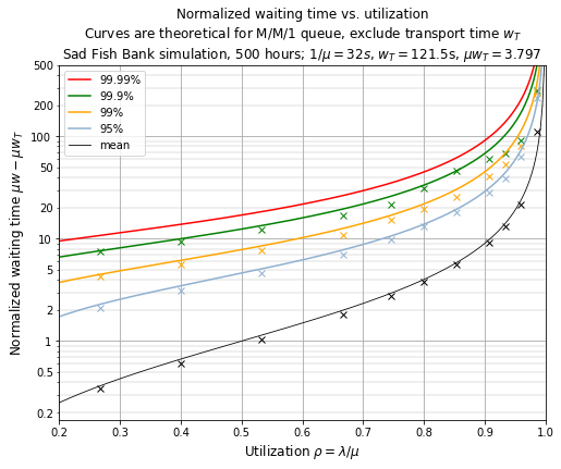
This graph plots normalized waiting times \( \mu w \): a value of \( \mu w \) = 1 is the same as the average time spent at the teller \( 1/\mu \) (32 seconds in this case). I have subtracted out the transport time \( w_T \).
The theoretical values of these times (mean waiting time, and waiting time for a given quantile \( q \))[27] are
$$\begin{aligned} \mu\bar{w} &= \frac{\rho}{1-\rho} + \mu w_T \\ \mu w_q &= \frac{1}{(1-\rho)}\ln\frac{\rho}{1-q} + \mu w_T \end{aligned}$$
which I have plotted in the graph above as solid curves, with measured values from 500-hour simulations of Sad Fish Bank shown as x’s. Again: the simulation measurements line up fairly closely with theory, until you get to very high utilizations.
This graph shows us the cost of trying to increase throughput. Theoretically we can run a bank or factory right near 100% utilization \( (\lambda=\mu) \), but the waiting time skyrockets. Increasing throughput increases latency, with very large sensitivity as throughput nears its maximum. If we want to keep our utilization at 80% (\( \lambda = \) 1.50 customers/minute) then we’re making customers spend an average of 4 times as long waiting for the teller as it takes the teller to process their requests — and in Sad Fish Bank, there’s another 3.8 times as long just making them traverse the large waiting space. Don’t you hate when there’s a big line in the airport that winds back and forth?
It would be much better if Sad Fish Bank could limit the customer arrival rate \( \lambda \), and limit utilization \( \rho \) to a lower value. This would reduce the waiting times — as well as cut the maximum queue length, which would allow Sad Fish Bank to use a shorter queueing area, reducing transport delays. At this bank, there are only a few ways to reduce utilization:
- turn away customers when they arrive too frequently (keep \( \lambda \) below a maximum)
- limit the number of customers allowed in the bank, turning away more customers once this limit is reached
- speed up the teller (probably not practical)
- hire more tellers (increase the service rate \( \mu \) — though technically when there are \( m \) tellers in parallel, the behavior is slightly different, forming an M/M/m queue instead of an M/M/1 queue.)
The down side of decreasing utilization (by hiring tellers) is that the bank is paying for resources to process customers. A utilization of less than 40% keeps the waiting time low, but try justifying to the bank’s Board of Directors that their tellers are spending most of their time waiting for customers.
The sum of the waiting time \( w \) and the service time \( x \) is the total system time \( s \), and the average normalized system time \( \mu \bar{s} \) is known as the X-factor in manufacturing, which is the normalized cycle time I showed earlier in the theoretical operating curve graph.
The X-factor is the ratio of total time needed to complete a manufacturing step to the raw processing time.* For example, if a widget waited 16 minutes for a machine that took 8 minutes to paint the widget, that would be an X-factor of \( (16 + 8)/8 = 3. \) An X-factor of 1 means that there’s no wait; cycle time is just the raw processing time needed to complete an operation. It’s possible to determine an X-factor for each machine as well as for the manufacturing process as a whole. X-factors in the 3 – 5 range are typical in semiconductor manufacturing.[28] This tradeoff of latency versus throughput is a tough one to optimize.
(*Fine print: raw processing time should really be considered as the theoretical minimum cycle time, and includes unavoidable delays such as transporting from one machine to another.)
Exponential Service Times, Revisited
I said earlier that the modeling of a bank teller’s service times by a Poisson process (exponentially-distributed) is kind of odd. Imagine a teller who is playing a dice game, throwing five dice every 1.16 seconds, and every time the dice shows a “full house” (three of one number, two of a different number), the teller processes the customer’s request instantly. Odds of a full house are 25/648, so this occurs on average every 1.16 × 648/25 = 30.07 seconds. Or another teller throwing five dice every 23 milliseconds, and whenever the dice are five-of-a-kind (odds \( =(\frac{1}{6})^4 = 1/1296 \)), the customer’s request gets processed, on average once every 0.023 × 1296 = 29.808 seconds. These dice game examples are essentially exponentially-distributed processes — although they are at discrete intervals, whereas a true Poisson process can have any interval of time between events, including 1 nanosecond.
Exponential distributions are very heavily front-loaded. Imagine ordering a grilled cheese sandwich from a diner with exponentially-distributed service times with a mean of 30 seconds. Your grilled cheese sandwich would arrive:
- 15.35% of the time, in less than 5 seconds
- 13.00% of the time, between 5 and 10 seconds
- 11.00% of the time, between 10 and 15 seconds
- 9.31% of the time, between 15 and 20 seconds
- 7.88% of the time, between 20 and 25 seconds
- 6.67% of the time, between 25 and 30 seconds
- 23.25% of the time, between 30 and 60 seconds
- 8.55% of the time, between 60 and 90 seconds
- 3.15% of the time, between 90 seconds and 2 minutes
- 1.58% of the time, between 2 and 3 minutes
- 0.21% of the time, between 3 and 4 minutes
- 0.03% of the time, between 4 and 5 minutes
- 0.0045% of the time, in more than 5 minutes

Very suspicious, indeed — and not very likely for processes that are consistent in nature. Some processes may have completion times that are exponentially-distributed in nature, like telephone calls, or time-to-failure for objects with constant failure rates. But constructing something?
Part of the reason M/M/1 queues, with their exponentially-distributed service times, are studied, may be like that old joke about the man looking for something under a street light:[29]
A few night ago a drunken man—there are lots of them everywhere nowadays—was crawling on his hands and knees under the bright light at Broadway and Thirty-fifth street. He told an inquiring policeman he had lost his watch at Twenty third street and was looking for it. The policeman asked why he didn’t go to Twenty-third street to look. The man replied, ‘The light is better here.’
The Poisson process is the easy case, and you can learn a lot just by studying it even if it’s not exactly what you need. (There are ways to analyze M/G/1 queues with more general service time behavior. Don’t ask me, though, unless it’s just citing basic formulas.)
The other reason to use simplified models based on exponentially-distributed service times is that they might not be that bad an approximation after all. Here’s why:
The Optimist’s Folly
Let’s look at a different random process that I call the Optimist’s Folly.
Suppose you have some kind of machine that processes its input in some time \( t \) consisting of a series of \( N=100 \) steps, each of which is some amount of time \( t_x \) which is either:
- \( t_x = T_0 = \) 0.2178 seconds with probability \( 1-p=0.999 \)
- \( t_x = T_0 + t_V \) with probability \( p=0.001 \), where \( t_V \) is random but uniformly distributed between 0 and \( T_1 = 164.38 \) seconds.
In other words, most of the time, the step takes exactly 0.2178 seconds; but about one out of a thousand times the machine has an intermittent failure which can take almost 3 minutes time to fix.
The mean time and standard deviation of the total time \( t \) are both 30 seconds, matching the mean and standard deviation of the exponential distribution for \( \lambda = 1/T \) where \( T= \)30 seconds. About 90% of the time, the machine doesn’t fail at all, and takes exactly 21.78 seconds to process its input.

The reason I call it the Optimist’s Folly is that most of the time this machine is faster than one which takes 30 seconds to complete its work. But every so often — about 10% of the time — it fails at least once, and unless you were very objective about determining its behavior, you would probably underestimate how quickly it finishes.
For those interested in the math:
This probability distribution doesn’t look anything like the exponential distribution… but queue behavior over a long time seems to depend on the sum of service times, making it subject to the Central Limit Theorem, which says basically that mean and variance are enough to characterize aggregate behavior of a large number of independent random quantities, and the quirky higher moments of their distributions disappear in the aggregate. (Imagine there are 10 people in line at a teller: the time for those 10 people to be processed is the sum of ten consecutive service times. This may seem trivial and obvious, but queue behavior also depends on how individual arrival times relate to those intervals when the queue is empty, and trying to apply the Central Limit Theorem to queueing theory is beyond my mathematical kung-fu.)
For example, here are the distributions for some assorted sums of service times taken from an exponential distribution and from the Optimist’s Folly distribution shown above:

With just one sample, the Optimist’s Folly has this bizarro probability distribution function (PDF) that kinda-sorta jumps around the corresponding exponential distribution, but with this big discrete bolus of 90.48% chance of being at time \( NT_0 = \) 21.78 s with no machine failures.
If we look at the sum of \( m=10 \) samples (ten teller service times added together) from the Optimist’s Folly, then the PDF kinda-sorta jumps around the corresponding sum of ten samples of an exponential distribution, called an Erlang distribution, and the discrete bolus makes up only 36.77% of the total at \( 10NT_0 = \) 217.8 s with no machine failures.
If we look at \( m= \) 30 or 60 or 100 or 150 then the overall sum of Optimist’s Folly service times has a distribution which more closely approximates the sum of exponential service times, and both tend toward a normal distribution with less and less differences at the tails as \( m \) increases. And the chance of having no machine failures drops like a rock.
Okay, enough with the probabilistic jabber; let’s see the Sad Fish Bank with the more realistic Optimist’s Folly process used in the teller:
In this simulation, the “real work” of the teller takes exactly 21.78 seconds, and a progress percentage is displayed. When there is a breakdown, the teller turns red, and the progress percentage stops; after it’s repaired, progress continues and the teller turns green again.
The graph below shows data from the Sad Fish Bank with Optimist’s Folly tellers, taken at various utilization ratios:

The mean waiting time \( w \) comes very close to the theoretical \( \mu w = \frac{\rho}{1-\rho} \) (after transport \( w_T \) has been subtracted) for both the Poisson and Optimist’s Folly processes: despite the fact that the service time distributions are very different for one sample, what matters most in the aggregate behavior of the queue is the arrival rate \( \lambda \) and the service rate \( \mu \) and the standard deviation of service time \( \sigma_x \). (For both the Poisson and the Optimist’s Folly behaviors shown here in the Sad Fish Bank simulation, service rate = \( \mu \) and \( \sigma_x = 1/\mu \), excluding the 2-second walk-up time.) The tails show slight differences, affecting the quantiles of 95%, 99%, 99.9%, but these differences aren’t very large as long as utilization \( \rho \) is not close to 1.
Generalized characterization
A Sad Fish Bank with constant-time teller servicing — this is called an M/D/1 queue with deterministic service times — reduces the normalized waiting time \( \mu w \) by half, with a mean value theoretically equal to \( \mu \bar{w} = \frac{\rho}{2(1-\rho)} \), shown as the dashed line in the graph above.
The generalized situation for both arrival and service times, where both have generalized probability distribution — is a G/G/1 queue, and the normalized mean waiting time \( \mu \bar{w} \) can be approximated by Kingman’s formula:
$$\mu \bar{w} \approx \frac{\rho}{1-\rho}\left(\frac{c_a{}^2+c_s{}^2}{2}\right)$$
where \( c_a \) and \( c_s \) are coefficients of variation of interarrival times and service times. These are just normalized measures of variability, equal to the standard deviation divided by the mean. For an exponential distribution, and for the Optimist’s Folly distribution, \( c = 1 \).
Note the two major factors here:
- the \( \frac{\rho}{1-\rho} \) part depends only on utilization \( \rho = \lambda/\mu \), the ratio of average arrival rate \( \lambda \) to average service rate \( \mu \).
- the \( \frac{c_a{}^2+c_s{}^2}{2} \) part depends only on how much variation there is in the arrival and servicing processes, and captures the “variability” factor of the operating curve graph I showed earlier. (Normalized cycle time = normalized waiting time + 1.)
For truly constant-time processes, \( c = 0 \): if you really know without a doubt that it takes exactly 30 seconds to process every customer and there are exactly 31.58 seconds between customers arriving, then even though the utilization \( \rho = 0.95 \), the waiting time for customers can be zero. But that’s a lot to assume, and rare events causing delays in the service time will increase both.
Math takeaways
That’s it for the heavy math in this section. What did we learn?
-
We looked at two very different mechanisms for service time of a bank teller: an exponential distribution and the “Optimist’s Folly” that describes an infrequent but long “downtime”.
-
Service downtime can be a significant source of variation.
-
When part of a queueing system, the exponential distribution and Optimist’s Folly have some behaviors that are very similar.
-
Aggregate performance measures like average waiting time vs utilization, or average queue length, depend almost completely on the second-order statistics (mean and standard deviation) of the probability distribution.
-
But the exponential behavior is easier to analyze!
-
We can substitute a real server (or machine) with an equivalent server that has exponentially-distributed service times — if we can characterize it!
-
Coefficient of variation \( c_x=\sigma_x/\bar{x} \) of some quantity \( x \), with standard deviation \( \sigma_x \) and mean \( \bar{x} \), is a useful and simple metric of variability, which can be used to predict statistical behaviors of waiting time.
-
Average waiting time \( \bar{w} \) for a single-server queue can be approximated with Kingman’s formula, where \( \lambda \) is the arrival rate, \( \mu \) is the service rate, \( \rho = \lambda/\mu \) is the utilization, and \( c_a \) and \( c_s \) are coefficients of variation for the interarrival and service times.
$$\mu \bar{w} \approx \frac{\rho}{1-\rho}\left(\frac{c_a{}^2+c_s{}^2}{2}\right)$$
-
Kingman’s formula tells you the average waiting time — but the waiting time has fluctuations, and can be several times higher on occasion. (For example, the Sad Fish Bank simulations show that one out of a hundred times it can be 5 – 10 times higher.)
-
-
The waiting time vs. utilization graphs zoom upwards as \( \rho \to 1 \), according to the \( \frac{\rho}{1-\rho} \) term in Kingman’s formula.
- The X-factor is the ratio of cycle time to raw processing time, and for typical semiconductor factories is in the 3 – 5 range.
Freddy’s Forgery Factory: A Follow-up
Here’s Freddy’s factory again — this time, we’ll compare what Freddy envisioned, versus a more realistic alternative where the machines have an Optimist’s Folly behavior for the same average processing rate of one canvas every 4.5 minutes (270 seconds). The inkjet and brush and inspection machines in “reality” take only three minutes and 16 seconds (196 seconds) to process, if the machines don’t break down. After taking the downtime into account, the net throughput capability is the same in both cases, envisioned and reality. But the variability caused by the downtime messes everything up. If you let it run for a while, you’ll note that Freddy’s factory in the “reality” case can’t handle canvases at a rate close to the expected factory capacity, and eventually the whole factory backs up.
In this simulation, the intermediate machines are colored according to their status in one of four ways:
- green: processing material
- white: waiting for incoming material to start processing
- red: downtime; machine is broken and needs fixing
- yellow: downtime; no space to unload outgoing material, and machine cannot accept any incoming material.
Green is good: progress is happening! Red and yellow are bad — no progress — as are extended periods of time where a machine is colored white, awaiting input from upstream sources.
One key thing to notice here is that there’s not much storage space if a machine backs up; the only place for canvases to go is on the conveyor belt, where there is room for four canvases between machines. So a downstream machine that breaks down can stop upstream machines from making progress, simply because there isn’t anywhere to put the canvases that finish upstream steps.
What if we added storage piles in between machines?
The factory which has storage has higher throughput, since WIP can accumulate and wait without blocking upstream machinery.
Reentrancy
There’s an important factor that affects semiconductor manufacturing lines, and that is reentrancy in the manufacturing flow. It’s not present in either Sad Fish Bank or Freddy’s Forgery Factory; the bank customers and canvases in the flow always go forward, never revisiting a past step. Semiconductor fabs, on the other hand, are heavily reentrant: each layer goes through many of the same steps, and when it’s time for the next layer, round and round the wafer goes again through the same machinery, a day or two later.
I don’t have a good simulation to show the effects of reentrancy, but let’s look at a thought experiment.
Marvin’s Maniacal Mini-Golf
Marvin Melville owns a miniature golf business in Malden, Massachusetts. It’s called Marvin’s Maniacal Mini-Golf, and it has four 18-hole mini-golf courses, each with a different theme: Cavemen, Conquistadors, Cowboys, and Cosmonauts. (Marvin drew heavily from his own boyhood fantasies; I wonder if he notices the effects of gender bias in his sales receipts.) Here is a map of the four courses:

In total, there are 65 holes. The reason it has 65 holes rather than 72 holes is that some of the holes are shared between courses.
- The 6th hole is shared on the north side by Cavemen and Conquistadors, and on the south side by Cosmonauts and Cowboys.
- The 12th hole is shared on the west side by Cavemen and Cosmonauts, and on the east side by Cowboys and Conquistadors.
- The 18th hole is shared by all four courses.
If it’s not too busy, it takes 40–45 minutes to finish each of the courses. Marvin’s staff would keep an eye on things, and if one of the courses was crowded, they’d recommend a less-crowded course instead. (The Conquistadors course always seemed to get the least interest from customers, something about the imagery.) Marvin’s rates were discounted for golfers who wanted to play more than one course: ten dollars for the first course, and seven dollars for each additional round. Occasionally someone would shell out the \$31 to play all four courses, usually frat boys from Boston.
One day Marvin got the bright idea for a promotion, called the Four-Leaf Clover: if you finished all four rounds in less than three hours, he’d refund most of the cost and only charge the ten dollars for the first hole. It brought in a bit more business. On slow days, sometimes people would finish in time, but Marvin wasn’t making a lot on those days anyway, and it seemed like his cost to run the promotion was outweighed by the fact that he was getting more people visiting his golf courses. When the weather was nice and things were more crowded, the Four-Leaf Clover promotion rarely paid out, because it was too hard to finish in time.
This worked well, up until a really crowded weekend in May, when one of the fraternity houses sent all their members to Marvin’s Maniacal Mini-Golf, and some of the frat brothers got into a fight, blaming each other for not moving fast enough so they could win the Four-Leaf Clover. The 18th hole was a big bottleneck, with a long line that filled up most of the nearby space, and that backed up most of the holes beforehand. The Cowboys course had delays all the way back to the first hole, and that meant that some of the people who’d finished the 18th hole on other courses had to wait to start the Cowboys course, and were not clearing out of the way quickly.
Gridlock.
Marvin’s staff quickly learned to limit the number of people on the courses if things got crowded, and warned customers not to try for the Four-Leaf Clover on those crowded days.
It’s no wonder things slowed down at Marvin’s Mini-Golf; this is an example of a reentrant flow, with cycles of slowness, and a major bottleneck at the 18th hole. If enough people are present, customers may find that they are blocking themselves from making progress more quickly. As a more precise example: if a golfer takes longer in the 7th hole on the first round, that can actually cause delays for the people behind them, including that same golfer in the second round.
But people find it easier to blame others; the more noticeable situation was for a group of mini-golfers seeking the Four-Leaf Clover to get started early, when there weren’t many people around, and then on the 3rd or 4th course, new people arrived and brought the system to a crawl.
Factories with non-reentrant flows avoid at least two effects that I can see. Without reentrancy, there is some limitation on things that can happen in the future. Sure, a machine might break down, and cause unforeseeable delays, but those delays are only going to happen once for the items in the line. The impact of slowness is dependent only on the section of line ahead of a given widget.
Let’s say we have two coffee mug factories, and for some reason, coffee mugs require 4 passes through a kiln.
- Factory A is non-reentrant and each coffee mug passes through four separate kilns: first kiln 1, then kiln 2, then kiln 3, and then kiln 4.
- Factory B is reentrant, and each coffee mug passes through the same group of kilns four times.
In factory A, if one of the kilns goes down for a little while, yes, it slows down traffic, and coffee mugs pile up, but the delays for a given coffee mug are limited to whatever lies ahead in line. Mugs are only impacted by the mugs and machines in front of them. If the factory manager decides to increase utilization, it won’t impact the cycle time of mugs that are already in the line, only the cycle time of the new mugs being started.
In factory B, if one of the kilns goes down and slows down traffic, the slowdown can go around and around the loop even after the kiln is repaired. If a bunch of mugs in batch #70301 pile up in their 2nd cycle, this can potentially delay the same batch of mugs in their 3rd and 4th cycles. Furthermore, adding too many new mugs in batch #70305 to the factory could delay batch #70301 on their 3th cycle, even though batch #70305 is “behind” batch #70301.
In essence, in a reentrant factory, WIP that’s not on its last cycle is behind itself and behind new products started later. That just hurts my brain to think about.
But You Already Know a Lot About Queues
I do have a few more minor things to point out — and bring this topic back to semiconductor fabs, of course — but I want to ground some of this talk of queueing in everyday reality. Whether you see them or not, there are queues at doctor’s offices and hair salons. We wait at restaurants to get a table, to order, to receive our meal, to pay for the check. Queues, queues, queues. At airports they are pervasive: we wait to find a parking space, to ride the elevator, to check our baggage, to get through security, to board the plane. Planes wait on the tarmac just to land or take off, because the utilization of runways at major airports is so high. (Want another Internet rabbit hole? Look up “airport slots” or “slot-controlled airports”.)

Queues are everywhere!
But the kinds of queues you will probably encounter on the average day are lines in a store and highway traffic.

If you are at a store — Svenskräp Import Goods, for example — and there are not many checkout lines open, or there’s a problem with some of the scanning machines, but customers keep arriving with more stuff, then the lines will get longer. At other times, the line lengths fluctuate; it’s all about random arrivals and how fast the checkout lines can service them.
Vehicle traffic is just as mysterious — and is probably the best everyday-world analogy to the ebb and flow of wafer traffic in a semiconductor fab. There’s a bunch of different queueing phenomena in a wafer fab that would be nice to observe and analyze, but the only people in the world with direct access are fab operations staff. Roadway and highway traffic, on the other hand, are such a common occurrence that almost anyone can study them, and it’s a lot easier to imagine cars stuck in traffic, than wafers stuck in traffic.
Here are some fab traffic effects mentioned in published literature (see the FabTime newsletters, for example, notably several issues in Volume 7):
-
short-term fluctuations caused by random variation in arrival and processing times
-
long-term fluctuations caused by overall increases or decreases in demand
-
increases in cycle time caused by…
-
randomness at high utilization
-
congestion at bottlenecks
-
local congestion caused by batching
-
single-tool paths through the fab
-
poorly-scheduled preventative maintenance
-
unscheduled maintenance
-
hot lots
-
high-mix fabs
-
All of these, more or less, have analogs in vehicle traffic.
Short-term traffic fluctuations
Sometimes roadways slow down to a crawl, and by the time the traffic movement picks up again, there is nothing to see, no accident or obstacle or lane closure. You have merely been a victim of random variations in traffic flow at close to the highway’s carrying capacity. As traffic flow increases, it becomes more turbulent, resulting in “waves” of traffic that speed up or slow down.
Some turbulence is visible in this photograph of traffic on Arizona Highway 202, which I showed earlier; the green outlined area has low density and the red outlined area has higher density. A few vehicles have brake lights on as they enter the higher-density zone.
If the traffic is heavy enough, these waves result in stop-and-go traffic.
Rush Hour: longer-term fluctuations in utilization
Both Freddy’s Forgery Factory and Sad Fish Bank presume an arrival rate that stays constant — unless you change it by moving the slider. Real-world queues are usually subject to some kind of fluctuation; during the day, banks and restaurants and highways and airports see lighter and heavier use, and as a result, the average queueing time changes. Sometimes the fluctuations follow patterns of rise and fall.

Traffic on eastbound Arizona Highway 202. Top: Sunday, 12:15pm. Bottom: Tuesday, 6:00pm.
I wanted to see how consistent traffic patterns were, so I tried an experiment.
Suppose you and a friend are running deliveries between a pair of supermarkets. One is the ShopRite supermarket in Hoboken, New Jersey, and the other is the ShopRite in Hauppauge, New York.

Travel between Hoboken and Hauppauge takes a little over an hour in light traffic. But it requires travel through New York City, which almost always has some congestion. How does it vary during the week?
I wanted to know the answer, so I used a traffic routing API from TomTom to capture some data. (TomTom’s API is free as long as you keep the number of requests below a threshold, currently 2500 per day.) I ran a program on my computer for about 10 months that made a pair of queries every 10 minutes to get traffic directions between the two ShopRite locations, and the results were enlightening. The traffic patterns are very strongly influenced by the time of day and day of the week, as you can see very easily from the graph below:

Some observations:
- Travel time is lowest during nighttime (departing between 8pm and 5am), presumably because fewer cars are on the road.
- During the day, travel time rises.
- On weekdays, there are two major peaks: one in the early morning hours, and one in the late afternoon hours. Travel time is lower on weekends, with only one gentle peak in the afternoon and early evening. This corresponds very well with the congestion caused by rush hour, as people go to work or return from work.
- Traffic on Thursday and Friday afternoons is the highest, reaching over twice the minimum travel time from Hoboken to Hauppauge.
- Hoboken-to-Hauppauge afternoon rush hour is more congested than Hauppauge-to-Hoboken, presumably because the dominant traffic patterns are commuting into New York City in the morning and exiting the city in the afternoon.
- Hauppauge-to-Hoboken morning rush hour is slightly more congested than Hoboken-to-Hauppauge, presumably for the same reason. Monday and Friday mornings are less congested than Tuesday, Wednesday, and Thursday.
- There are occasional anomalies from these patterns, notably:
- congestion from Hoboken to Hauppauge around midnight on some days.
- lower travel times on holidays (the lowest Monday and Friday afternoon travel times were on holidays: February 20 = Presidents’ Day, July 4 = Independence Day, and November 25 = the day after Thanksgiving)
- on Friday, September 9, 2022, there were traffic delays from around 7am - 9am departing Hauppauge to Hoboken. I am not absolutely certain of the cause, but this was during the U.S. Open tennis tournament in Flushing Meadows.
Transportation professionals use all sorts of performance metrics (called Measurements of Effectiveness, or MOEs by the US Department of Transportation) to evaluate traffic conditions over the long term, so they can make plans to mitigate the worst conditions — whether by highway widening or other means. Some of these metrics include measuring at a certain percentile, say the 90th or 95th percentile during a particular month of travel time, or its difference or ratio to the average time.

Figure 3 from US Federal Highway Administration, "Travel Time Reliability: Making It There On Time, All The Time"
This percentile-based approach near the worst-case peak is an important method to determine the impacts of capacity: even if the average travel delays are low, the decisions made to widen a highway will be based on its performance metrics under heavy traffic.
Smooth traffic flow (or lack thereof)
Most of the other causes of traffic congestion arise from anything that gets in the way of smooth traffic flow.
Traffic congestion occurs at merging bottlenecks — for example, a place on the highway where the number of lanes decreases from three to two, or a section of road under construction, or an on-ramp at an interchange.
The location I took these pictures of Arizona Highway 202 was more interesting than I had expected. This was near a metered on-ramp:
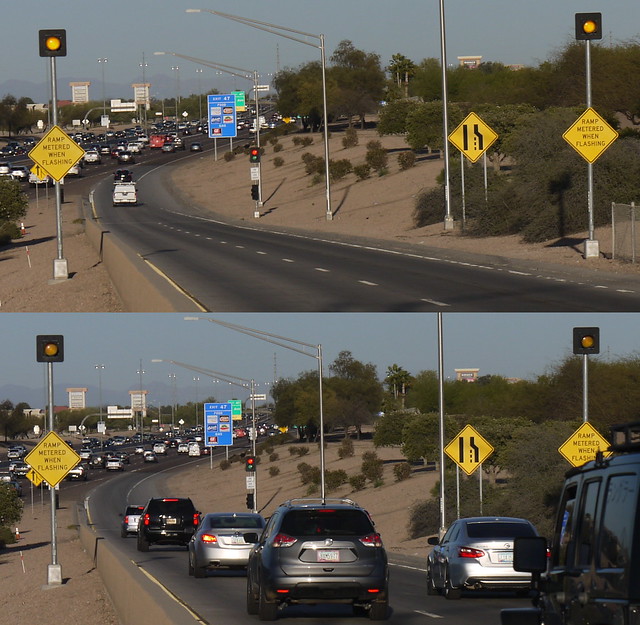
Arizona Highway 202, eastbound on-ramp at 6:03pm on a Tuesday. The bottom picture was taken 16 seconds after the top picture.
During rush hour, the on-ramp can fill up fast, because the traffic feeding it isn’t a steady flow: when I was there, most of it came from a left turn lane at a traffic light, so when the left-turn light turns green, all of a sudden all of the cars waiting at the light have a chance to enter the on-ramp. The light at the bottom of the on-ramp turns green to signal the next car to proceed, about once every few seconds. This smooths out the traffic flow onto the highway.
From Florida’s Department of Transportation:
Ramp Signals are traffic lights that reduce congestion along northbound and southbound Interstate 95 (I-95) in Miami-Dade and Broward Counties.
Ramp Signals are activated during times of heavy congestion, such as weekday rush-hour periods, but may also be activated in case a traffic incident or special event impacts regular expressway operations. The signals work based on real-time traffic conditions and alternate between red and green lights to control the rate which vehicles enter the highway. They break up the groups of merging vehicles to reduce the impacts of entering traffic to regulate the flow on the mainline. To date, Ramp signals have significantly improved mobility and travel speeds during the evening and morning rush hour periods by 16% and 11% respectively.
Without the smoothing effect of metered on-ramps, a surge in vehicles entering the highway is likely to create a burst of local congestion as they merge. In heavy traffic, such bursts propagate as waves, [30] affecting not only the cars in the immediate vicinity, but all cars behind them.

Another quirk of road or highway traffic is the presence of emergency vehicles (police cars, fire engines, ambulances) which have priority over other vehicles. The emergency vehicles can get through traffic faster — with the cost of slowing down everyone else.
In cases where there is only one lane in each direction, and passing is not allowed, a slow vehicle makes everything behind it slow. Two lanes allow traffic to flow around a slow vehicle.
In fact, traffic would be a lot smoother, and therefore less prone to congestion, if all the vehicles were the same, with the same driving habits. That is not reality, unfortunately; we have fast vehicles, slow vehicles, large vehicles that take up more than one lane (wide loads), small vehicles that dart between lanes (motorcycles), slowly-accelerating vehicles (medium- and heavy-duty trucks), vehicles that stop at all railroad crossings (school buses and vehicles carrying certain types of hazardous materials), vehicles that stop frequently (buses)… it’s a mess.
Now imagine a road network with a hodgepodge of vehicles: sportscars, school buses, slow-moving farm equipment, trucks carrying modular homes, cement trucks, dump trucks, tractor-trailers, motorcycles, police cars, ambulances — all of which are going around a city in several loops that intersect or merge into each other. There are railroad crossings and steep hills. Add a dozen street sweepers combing the city to clean off all sections of the road network at least once every 72 hours, and a bunch of areas where lanes are closed for repaving or other construction, with detours. In some cases the road is reduced to one lane, and highway flaggers give the go-ahead for alternating caravans, one direction at a time.
Don’t forget the occasional vehicle crash.
Now you’re ready to think about traffic delays in a semiconductor fab.
Fab traffic
As I mentioned, most of these queueing phenomena affecting highway and road traffic also affect semiconductor fabrication:
- short-term fluctuations caused by local variation in arrival and processing times, and can lead to “WIP bubbles” (local accumulations of WIP waiting in front of a tool, similar to traffic waves)[31]
- long-term fluctuations caused by overall increases or decreases in demand (similar to seasonal variation in traffic) — there are some semi-regular patterns in these fluctuations, including the four-to-five-year industry cycle, the surge in USA consumer electronics demand leading up to Christmas, and delays caused by staff vacations in Europe in summertime and in the Far East during Lunar New Year.[32]
- congestion at bottlenecks (similar to highway merges)
- local congestion caused by batching, where a tool operates on and releases several wafers at once, causing alternate decreases and increases in downstream traffic (similar to traffic downstream of a stop light)
- mitigation of batching through gradual release of wafers (similar to metered on-ramps)
- increases in cycle time caused by lots of wafers that have higher priority, known as “hot lots” (similar to emergency vehicles)
- single-tool paths through the fab are much more vulnerable to congestion than places where multiple tools operate in parallel (similar to highways with only one lane in each direction, compared to those with multiple lanes)
- increased variability due to product mix — some fabs focus on high-volume products such as DRAM or high-end microprocessors, and can keep the same sequence of steps; in others, notably foundries and IDMs with a wide product base, the different products have to share the same equipment, but require different setups and different sequences of processing steps, making it harder to achieve smooth flow through the fab (similar to traffic turbulence caused by lots of different vehicle types sharing the road)
The batching issue is subtle, and deserves a short discussion.
Batch tools
Earlier in this article, I noted that the cycle time in the ideal version of Freddy’s Forgery Factory was approximately 123 minutes and 30 seconds, whereas Freddy calculated 94 minutes, an underestimate of about 30 minutes.
This ideal model doesn’t have any variability caused by machine breakdowns. But Freddy overlooked something important in his calculations, namely that a batch tool may cause increased queueing before and after the tool. In Freddy’s case these are the two aging ovens.
Oven 1 and Oven 3 each take 18 minutes to process a batch of four canvases. The ovens wait until they have a full batch before starting. This leads to downstream grouping of the canvases in batches of four. In the screenshot below, canvases 16 – 19 are part of one batch which recently finished processing in Oven 3; 20 – 23 are part of another batch in process in Oven 3; 24 – 27 are part of a third batch lining up for Oven 3; and so on. At the instant captured, canvas 24 is just arriving in place to wait for Oven 3.

The last canvas in each batch (19, 23, 27, etc.) arrives at Oven 3 right in time for the oven to start, without any delay. But when the oven finishes, and all canvases in the batch are released, it has to wait in a queue in front of final inspection for the other three canvases to complete before it can start. That’s an extra 5 minutes per painting, or 15 minutes.
The third canvas in each batch (18, 22, 26, etc.) has to wait 5 minutes at Oven 3 for the fourth canvas to arrive, and has to wait 10 minutes at final inspection for the first and second canvases in each batch to complete before it can start. Total wait in queues: 15 minutes.
Not surprisingly, the total wait for the other two canvases is also 15 minutes:
| Batch position | Wait time Oven 3 | Wait time Inspection | Total |
|---|---|---|---|
| First (16, 20, 24, ...) | 15 m | 0 | 15 m |
| Second (17, 21, 25, ...) | 10 m | 5 m | 15 m |
| Third (18, 22, 26, ...) | 5 m | 10 m | 15 m |
| Fourth (19, 23, 27, ...) | 0 | 15 m | 15 m |
The canvases move one place forward if we let Freddy’s Forgery Factory run another five minutes:

(In this case 4 minutes 45 seconds have elapsed between the screenshots: canvas 25 is just arriving in place to wait for Oven 3. When canvas 24 moves into the oven, it will take another 15 seconds for canvas 25 to move to the end of the conveyor belt before loading into the oven, for a total of 5 minutes delay at Oven 3.)
Oven 1 is similar, but the wait there depends on the times between canvas starts. With 11.8 canvases per hour, the starts are approximately 305 seconds (5 minutes 5 seconds) apart:
| Batch position | Wait time Oven 1 | Wait time Inkjet | Total |
|---|---|---|---|
| First (16, 20, 24, ...) | 15:15 | 0 | 15:15 |
| Second (17, 21, 25, ...) | 10:10 | 5 m | 15:10 |
| Third (18, 22, 26, ...) | 5:05 | 10 m | 15:05 |
| Fourth (19, 23, 27, ...) | 0 | 15 m | 15:00 |
The two ovens together contribute between 30 minutes and 30:15 of extra queueing, depending on the position in the batch, in addition to the 94 minutes in Freddy’s calculations. So the total cycle times should be between 124 minutes and 124:15.
The remaining discrepancy is 30 seconds off from the measured cycle times — I’m sure there’s a reason, but when you’re accounting for effects like this, at some point you just have to walk away and be happy you’re close enough.
(Another error in Freddy’s calculations cancels out. The machines simultaneously load and unload a canvas, so that the new one slides in as the old one slides out. Freddy took load/unload times into account from the perspective of the machines, not from the perspective of the canvases. So the inkjet machine, for example, which takes 4.5 minutes to process a canvas and half a minute to do the unloading/loading, has a throughput bottleneck of 5 minutes per canvas. Each canvas, on the other hand sees unloading and loading as separate operations, taking half a minute each, adding up to 5.5 minutes spent at the inkjet machine from the canvas’s perspective. But the unloading time is already counted as part of the 60 second conveyor belt transport time between machines. If you slow things down to actual speed, and count carefully, it takes exactly 60 seconds from when the inkjet machine finishes, and starts unloading a canvas, to when that canvas arrives in front of the brush machine and starts loading.)
Another method of approximating the extra 30 minutes delay caused by batching is to notice that there are 6 canvases that are waiting in queues before and after the two ovens, which adds another 5 minutes each of WIP. There’s Little’s Law again: equivalence between extra WIP and extra cycle time.
One way of mitigating some of the extra queueing in batch tools is not to wait until the tool is full, and start whenever a reasonable amount of WIP arrives. For example, Freddy could start each oven after loading whatever canvases are present when the oven becomes free, without any further waiting. This works at low utilization, but at high utilization, it just means that the canvases have to wait until the oven is free, with those arriving earlier waiting longer. And when the oven does contain a full batch, the batch is released downstream, with those arriving later having to wait longer for the next tool.
If batch tools are inexpensive, another way to reduce cycle time is to have several of the same tool, operating with staggered starts. Imagine a bus route with dozens of buses, arriving one minute apart and picking up whichever passengers are present at the stop. This would reduce passenger waiting at bus stops to a maximum of one minute. It costs a lot of money to run all those buses, though.
We can actually try this sort of effect in action in a simulation.
Red Laser Bakery
Welcome to Red Laser Bakery, home of the world’s only laser-accelerated manufacturing facility of pastries and breads.
Red Laser Bakery’s baking process consists of two cascaded pairs of a group of ovens and a laser station.
Each oven can run a batch of up to 12 trays. This takes 40 minutes for many breads and pastries. A group of ovens is followed by a laser station, which can process one tray at a time, heating a thin crust on the outside of the bread or pastry. The laser station is very fast but breaks down frequently, creating an Optimist’s Folly servicing process with a mean and standard deviation of approximately 2 minutes. The ovens are low-tech and reliable.
The bottleneck of Red Laser Bakery is the laser station, which can handle an average of 30 trays per hour. Initially the bakery used a group of two ovens, with a maximum throughput of 2 × (12 trays / 40 minutes) = 36 trays per hour, starting any oven every 30 minutes when at least one tray was present.
After some analysis, the bakery decided to double the number of ovens, leading to a maximum processing capacity of 72 trays per hour, starting any oven every 15 minutes when at least one tray was present. The bakery staff found that this lowered cycle time by about 20 - 25 minutes for almost any level of utilization.

The decrease in cycle time is significant because the time in the ovens is such a large part of the overall process time, and because the trays incur extra queueing time while waiting for ovens to start each batch.
Batch tools in semiconductor fabrication
Fabs have lots of tools with batching behavior, which makes it more challenging to control cycle time. I quoted a section of Mason & Fowler’s paper earlier:[25]
Typically, the individual silicon wafers upon which semiconductors are manufactured are grouped into “lots” of 25 wafers. Each lot is uniquely identified in the wafer fab’s manufacturing execution system (MES) as a unit of production (job). Therefore, the individual wafers within a lot travel together throughout the manufacturing process.
The equipment set used to manufacture semiconductors is typically made up of 60 to 80 different equipment types. These equipment types contain a diverse array of wafer processing tools in terms of the quantity of wafers that can be processed concurrently. While single wafer tools (photolithography steppers) only process one wafer at a time, other tools (acid bath wet sinks) can process entire lots concurrently. Wafer fabs also contain batching tools (diffusion furnaces) that can process multiple lots of wafers simultaneously.
Whether the wafers in a lot are processed individually or concurrently, they are still processed as a group. The fastest lithography tools can process between 200 and 300 wafers per hour,[33] which means that one wafer can complete an exposure in as fast as 12 seconds. Other processes such as chemical vapor deposition (CVD) can have similar throughput.[34]. With lots of 25 wafers, the entire group must be processed before proceeding to the next tool, so that the 12 seconds per wafer turns into 300 seconds per lot. On tools that process an entire wafer lot concurrently, this is the time for the whole lot to complete; on tools that process one wafer at a time, most of the time is spent waiting for the rest of the lot to complete. Multiply by a bunch of different types of tools, and add time to transport and load/unload, and the waiting time adds up. (Also: the vendor-provided throughput rates, like 200-300 wafers per hour from lithography tools, are while the machines are running. Preventative maintenance and unscheduled downtime eats into that throughput significantly.)
One way of reducing cycle time is to combine individual tools into a cluster tool, as shown below. Cluster tools accept a wafer lot through load locks, either manually, in the case of older fabs, or by a transfer robot from a FOUP in a loading station, in the case of newer fabs with automated material handling systems. Once the wafer lot is loaded, a vacuum can be applied and one or more wafers from the lot can be transfered to individual processing chambers. This allows the group of wafers to be processed in a pipelined manner, so that it can visit each process in the cluster, without having to wait for the rest of the lot until the end of the sequence. Many cluster tools have two load locks, to allow loading of a second wafer lot while another lot is under way.

Diagram of a cluster tool, edited from Figure 1 of Chung-Ho Huang et al., 2020 (U.S. Patent Application 20220206996A1)
Some steps in the fab, such as oxidation or diffusion, require use of a high-temperature furnace. These steps can take hours to complete. To achieve higher throughput, furnaces can process a large batch of several wafer lots concurrently — with the tradeoff of increasing cycle time when incoming lots queue up for the furnace, and when outgoing lots released together may queue up at the next tool.
If enough furnaces are available, it may be possible to run smaller batches, reducing queue time.


Top: Four-stack horizontal furnace. Bottom: A batch of four lots (100 wafers) unloaded from a furnace.
Photos by Colin Wilson, Expertech, used with permission.
This gets into the question of capacity planning: is it better to add equipment that increases maximum throughput, or equipment that helps decrease cycle time? At Red Laser Bakery, the increase in ovens helped reduce the cycle time, but didn’t do much for throughput. Here’s a couple of different scenarios for capital improvements:
- Leave lasers unchanged, add two ovens
- Upgrade lasers so they are 5% faster, add one oven
- Upgrade lasers so they are 10% faster, leave ovens unchanged
Which is best? They generate different operating curves:

At high utilization, upgrading the lasers (improvement 3) is best, since it pushes out the asymptotic rise in cycle time as throughput approaches maximum capacity. At low and mid-range utilization, adding ovens (improvement 1) is best, because maximum capacity isn’t very relevant. Improvement 2 provides across-the-board improvement that is in between the other two proposals.
To get a sense of which is the ideal set of improvements, we’d have to know more about how heavily loaded Red Laser Bakery plans to run, how much the equipment costs, and how much of an impact cycle time has on Red Laser Bakery’s operations — as well as some idea of a good optimization methodology, which I don’t have. At this point, the usefulness of studying a fictional bakery breaks down.
Fabs in the Real World
There are essentially two kinds of published accounts of what goes on inside a semiconductor fab. One is mainstream media coverage, aimed at the general reader, and the other consists of academic and trade journal articles. Both can be enlightening, but not greatly so.
Mainstream media accounts tend to give a better flavor of what it’s like in a wafer fab — but because of the semiconductor industry’s proprietary nature, these tend to be focused on two aspects in particular:
- impressiveness: the fact that a semiconductor fab is really high-tech, complicated, clean, and expensive
- education: the general nature of the steps used in the wafer manufacturing process (lithography, etching, etc.)
Here are two examples of those; I’ve listed some more in the References section.
One is the Commodore Computer / MOS Technology factory video from 1984, which I mentioned in Part Two. This is historical in nature, with most process steps handled manually by fab operators, and the video leans toward the educational aspect.
The other is John Burek’s September 2022 tour of Intel’s Fab 28 in Kiryat Gat, Israel, for PC Magazine.[35] This leans toward the impressiveness end of the spectrum.
I love impressiveness. I could watch Intel’s video on its automated material-handling system (AMHS) over and over again. It’s wonderful seeing all these numbered robot vehicles zooming around the overhead rail system — look, there goes number 529! — and then occasionally, like some high-tech mythical ninja monster, a robot shoots down a plate lowered by motorized belts, which grabs hold of a FOUP and snatches it up to resume its journey through the fab. You definitely get a flavor of what it must be like to be inside a state-of-the-art wafer fab… the yellow lighting in the exposure area; the cleanroom suits; wafers being carried around at high speed, never handled by human beings; and so on.


Top: Overhead hoist transport vehicles. Bottom: Up, up, and away! A vehicle hoisting up a FOUP.
From Intel's Automated Superhighway: 'The Heartbeat and Blood Flow of the Fab' (Credit: Intel Corporation)
As an engineer, I crave learning more than this. Occasionally there are little snippets of information: Burek and his fellow journalists must use special notebooks in the fab, which are engineered not to produce paper dust, and have pages printed with “low-sodium ink for reduced ionic contamination.”
Commodore’s factory video also has little snippets about the fab, and is useful for comparison. Here there are horizontal furnaces for diffusion; about 14 minutes in, the video shows a worker placing four quartz “boats” onto a cantilever arm that loads the wafers into a furnace. The video mentions (in German) that the diffusion furnace takes about three hours. There’s a short close-up of a quartz boat, and if you count carefully, you can see that there are 38 wafers. (These are likely four-inch wafers.)


Top: Worker loading wafers onto a furnace arm. Bottom: Close-up of a quartz boat holding wafers that have finished diffusion processing.
From 1984 Commodore Computer factory tour video
But the details are few. WIRED has published a couple of fab tour articles; a 1994 visit by Rudy Rucker to an AMD fab[36] states that “getting a hundred 486 or Pentium chips onto a silicon wafer involves laying down about 20 layers” and “the process takes as long as 12 weeks for a completed wafer’s worth of chips”. (That would be up to 4.2 days per mask layer, which seems rather high.) Rucker also visits an Intel fab, and notes that wafers are transported manually at AMD, but by overhead vehicles at Intel: “a miniature overhead monorail on which the boats move about automatically”. He also briefs us on fab terminology of a bay-and-chase cleanroom:
The layout of a fab is a single main corridor with bays on either side. To keep the bays clean and uncluttered, most of the machines are set so that their faces are flush to the bay walls, with their bodies sticking out into sealed-off corridors called “chases.”
A more recent WIRED article from March 2023 chronicles Virginia Heffernan’s visit to a TSMC fab in Taiwan,[37] and reveals… almost nothing about the fab. The article, titled I Saw the Face of God in a TSMC Semiconductor Factory, is more of an essay, talking about the geopolitics of semiconductors in Taiwan, and the author’s sense of religious joy at being invited into this holy temple of technology:
At the sight of the lithography machine, my eyes mist. Oil, salt, water—human emotions are shameful contaminants. But I can’t help it. I contemplate, for the millionth time, etched atoms. It’s almost too much: the idea of tunneling down into a cluster of atoms and finding art there.
I want to scream. WIRED, you got once-in-a-lifetime permission from TSMC for one of your journalists to visit one of the world’s most sophisticated wafer fabs, and you let her describe it in spiritual terms?!?!! Bah!
I did find one published account of a fab visit that has some real meat to it, and is relevant to discussions on cycle time. In 1996, journalist Helen Thorpe from the magazine Texas Monthly visited Motorola’s MOS 11 plant in Austin,[38] writing about typical workdays in the fab, and sprinkling all sorts of interesting details, from the lint-free notebook and low-sodium pen she was required to use (“The sodium in the ink of a normal ballpoint pen can paralyze a factory because it can become a charged ion, travel through the air, and alter the electrical properties of the wafers it lands on.”) to operations briefings:
One morning, Steve Brown, the supervisor of the factory’s first shift, sketched what had happened the day before. “Yesterday the WIP was 31,559,” Brown told the other managers, referring to the “work in process,” or the number of wafers going through the factory. “And we did 63,130 turns.” In other words, every wafer had moved through an average of two steps in the assembly process—the industry’s equivalent of breakneck speed. Brown described problems that were likely to impede the flow of wafers through the factory that day: Two fifths of the factory’s low-temperature furnaces weren’t working; one of the machines that check the dimensions of circuits was down; four fifths of the machines that perform a crucial process in an area called etch were out of commission; and an unwieldy bulge of wafers was converging in an area known as diffusion. “A lot of inventory has slammed into there recently,” warned Brown. But MOS 11’s managers cultivate a macho, matter-of-fact presumption that problems will be solved, so nobody seemed alarmed. “No real major issues are expected,” Brown concluded. “We should have a pretty good day.”
Thorpe somehow gives an account of various process steps (dry etch, sputtering, ion implanters) that are both accessible to the nontechnical reader, and also interesting and full of factoids to tech nerds like me. She recounts a few key details about process durations in MOS 11:
- cycle time: 40 to 80 days
- number of layers: as many as 50 (note: that works out to 1.6 days per mask layer)
- the fab produces PowerPC processors, which have twice as many steps as other chips made in the same fab, and lower yields (she cites one wafer that had a 20% yield)
Yes, this article is nearly 30 years old, but it still seems relevant and informative.
I would like to say something more definitive about the way a semiconductor fab works — but I can’t. The only first-hand experience I have is a visit to Microchip’s Fab 2 in Tempe, Arizona, last year. It reminded me of a very high-tech laundromat. Silicon wafers are being washed or etched inside rows of machines set into the wall, waiting for the machines to finish so they can be unloaded and moved somewhere else, and more wafers loaded in their place for the next run. The main noise is the whoosh of air circulating through the clean-room filters.
For some reason, I was expecting workers to be rushing around hurriedly — but their motions were very deliberate, lifting wafer carriers deftly and placing them in a box or loading them into the next tool, with a great deal of care to avoid any sudden jostling or acceleration, as befits a fragile and valuable work in process.
Because the production process goes through so many steps that take hour after hour, it’s not possible to observe a sense of “flow” through the factory, like the beer-bottling machinery or my visualizations of Freddy’s Forgery Factory and Red Laser Bakery and La Banque du Poisson Maussade. Some of the patterns that indicate delays or the beginning of unexpected bottlenecks in a wafer fab are probably visible only to fab operations managers tracking the progress of wafer lots. I have asked several fab workers at different companies about how often machines go down; the answers I’ve received are rather vague, perhaps deliberately so. Anyway, with hundreds or even thousands of tools in a typical semiconductor fab, the chances of at least something going awry on any given day are fairly high. Unscheduled tool downtime is allegedly the major cause of variability in fabs.[39]
Academic / trade journals
The other type of published account of semiconductor fabs is through academic or trade journals; these tend to be more specialized, and spend very little time talking about what a visit to a fab feels like, and get straight to the point — which is good for getting technical information, but if you have no idea what a fab is like, it can be really hard to figure out what they’re talking about. (Also, because the industry is very proprietary, few real details are disclosed.)
Most of what I’ve learned about the way factories and fabs work in the real world comes from a few written sources I’ve listed in the References section — notably the FabTime Inc. newsletters, which are an amazing resource for anyone wanting to learn about how semiconductor fabs manage cycle time. Factory Physics by Hopp & Spearman is a good place to start, as well.
There are also a few crumbs of information about process times scattered around in various published accounts. Here are a few of the ones I’ve been able to find:
-
Peter Gaboury of STMicroelectronics wrote an article published in Future Fab International in June 2001[40], including these statistics:
-
Graphs of average processing times for two stepper exposure tools (a 350nm I-line stepper, and a 250nm DUV stepper) against the wafer position in a lot, showing the first wafer takes much more time, perhaps for additional setup

Redrawn from Figures 6 and 7 of Gaboury 2001[40]
-
Metal etcher: 311 sec average processing time, 434 sec standard deviation
- Single wafer medium current implanter: 35 sec average processing time, 92 sec standard deviation
-
-
Donald Martin at IBM published a paper in 1998 on X-factor with this bit (my emphasis):[41]
Tools with raw process times of less than a half hour tend to have significantly higher X-factors than tools with raw process times greater than a half hour. This difference results when the shorter raw process time tools are effected, for example, by transportation and staffing issues more than the longer raw process time tools. For a six-hour furnace operation, the effects of lunchbreak are insignificant on the X-factor; as opposed to a 20-minute ion implant, where lunchbreak can significantly impact the X-factor. Therefore, the customization of X-factor targets by individual tools/toolsets, while still maintaining the overall line X-factor objective, is of crucial importance.
OK, so Martin never actually says that IBM’s furnace operation takes six hours or that IBM’s ion implant takes 20 minutes, but why would he make up totally unrealistic numbers? So presumably the process times in a real fab were roughly the same order of magnitude. Martin goes on to mention another example:
The use of the X-factor contribution analysis for a semiconductor manufacturing line is shown in Figures 5, 6, and 7. Figure 5 shows the line aggregated into 12 major departments, which include all tools being run by each department. In this case, it is clear that the department called WETS has the largest X-factor contribution for the entire line. Figure 6 shows that of all the tool types being run by this department, ARCPS tools have the greatest X-factor contribution. Finally, Figure 7 shows that within all the ARCPS tools, the four tools dominate the performance of the tool set.

Contributions to X-factor, redrawn from Fig 5 of Martin 1998[41]
Figure 7 of Martin’s paper shows that ARCPS tools have an X-factor contribution that is five times larger than the next-largest toolset (CFM), and much higher than other WETS tools (CURE, FSI, STI). Apparently WETS = wet bench tools for etching and cleaning: ARCPS, CFM, FSI, and STI were all different manufacturers of semiconductor wet bench equipment in 1998. But it looks like one vendor’s tools (ARCPS) were the culprit in this case, and there’s not much we can learn about what contributes most to fab cycle times in general from this example.
-
Some engineers at Skyworks Solutions published a conference paper in 2018 that mentions the case study of an unnamed fab (presumably one of Skyworks’ fabs) tracing cycle time problems in photolithography:[42]
However, the cycle time started increasing after several weeks of output. The local IE team performed a cycle time pareto analysis similar to what was displayed in Figure 5. This data indicated that the factory’s photolithography area, mainly the steppers, was performing at 8X its theoretical cycle time. Review of previous month’s data showed that the cycle time alone at the steppers had increase by a factor of 250%.
This paper goes on to show a graph of Canon photolithography stepper utilization in the 85-90% range, and states that by analyzing logs in the fabs, the industrial engineering staff were able to conclude that degraded components were slowing down throughput:
The tools were not performing at the same speed as they had been and it was deemed that in order to maintain higher output, these components should be changed out more frequently for the benefit of throughput. By being able to identify the root cause of the issue, the queue time that had been accumulating in the photolithography area was brought back into control and the factory was able to meet the cycle time requirements again.
Aside from the photolithography utilization, the paper doesn’t reveal any absolute numbers.
-
A 2013 paper by Intel staff[43] shows some ion implanter process time correlations with wafer slot in a 45nm fab:

Redrawn from Kalir 2013[43]
-
A 2018 conference paper written by staff at Axcelis Technologies describes some process details for the company’s ion implanters:[44]
Modern ion implanters run in production at around 30mA beam current for a typical low energy Phosphorus implant and so an implant time of around 1.5 minutes per wafer may be considered typical for these experiments. Due to the dose, the implants are not mechanically limited and run at a factor of 10 below the 500 wph mechanical limit — as a result, wafers spend a considerable amount of time staged awaiting implant.
(Note that ion implanters have come up several times, with some variation in the numbers but conceivably in the same order of magnitude: Axcelis lists 1.5 minutes (90 seconds) per wafer; ST’s Gaboury listed 35 seconds; the 2013 Intel paper shows something in the 60-80 second range; whereas Martin’s 1998 paper mentions 20 minutes, although perhaps this is per 25-wafer lot, making it 48 seconds on average per wafer.)
-
A 2018 journal paper by engineers at SilTerra about WIP management[45] summarized various sections of a fab process. It’s not clear whether these are actually from one of SilTerra’s processes or a made-up simulated process. (SilTerra is a foundry, but, unlike TSMC, has maintained a set of process technologies primarily from 180nm to 110nm for the last ten years or so, without following Moore’s Law any further.) In either case, however, the perspective is insightful; the authors describe a typical 37-layer process in 7 groups as part of a “zonal WIP management” strategy, pointing out some key differences between the groups:
2.1. PrePoly One (PreP1)
PreP1 started from wafer loading to the Nitride Strip process. With average 4 masks level a longer CT is expected at Prep1 due to reentrants for Diffusion Furnace process. Diffusion is a batch process and the process duration from 8 to 12 hours. PreP1 has 6 Diffusion steps.
2.2. PrePoly Two (PreP2)
PreP2 started from HNWell Mask to Pwell Implant Resist Strip process. PreP2 typically has 10 mask layers mainly the reentrants for Implantation process. The wafers typically moves between Photolithography, Implant and Cleaning. Wafers are moving fasters at this area even though Photolitography is the bottleneck for the FAB.
2.3. Poly
Poly module started from Gate Oxidation 1 or MV Gate Oxidation process to Poly Etch process. Poly typically has 3 mask layers. Poly also consist 4 Diffusion Furnaces step. Due to the longer furnaces process, the process cycle time at this area is designed to be longer.
2.4. Post Poly 1 (PstP1)
PstP1 started from the NLDD Mask layer to Spacer Nit Etch. PstP1 also has 8 Implants step with 5 mask layers. The theoretical cycle time is shorter and will generate fast WIP turn.
2.5. Post Poly 2 (PstP2)
PstP2 started from NSD mask layer to ILD CMP process. PstP2 has 3 mask layers. Consist of 3 Implant mask layers and multiple thin film deposition layers. It is also consist 1 Chemical Mechanical Polishing (CMP) layer.
2.6. Backend (Backend)
Backend started from Contact Mask to Top IMD CMP. Backend has 9 mask layers and multiple re-entrant processes between Photolitography, Etch, Thin Film and CMP. Backend is single wafer processing type of tools. Theoretical Cycle time is faster at backend.
2.7. Final
Final started from Top Via Mask to Shipping. Final has 3 mask layers. The completed processed wafers required to run through electrical test process. Wafer Acceptance Test (WAT) is a routine run test for every wafer where the wafer will be electrically tested. A test structure is designed at the scribe line to electrically confirm our process. Good wafers will be thoroughly inspected by the Outgoing Quality Assurance (OQA). If there are no abnormalities found, the good wafers will be packed and ready for shipment to the customer’s location.
The authors also state that wafer fabrication “is typically from 45 to 60 days” and “may need to visit photolitoghraphy [sic] module 20 to 38 times for all layers of circuitry to be fabricated.” (This implies on the order of 1.5 - 2.3 days per mask layer.)
They include a figure that shows one way of visualizing the WIP in the fab through these layers:
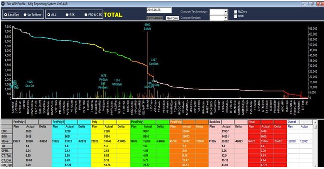
Cumulative WIP profile, arranged by process step. Figure 6 from Dynamic WIP Management with the BullWIP Situation for Semiconductor Fabrication Foundry,[45] by Mohamad Zambri Mohd Darudi et al., used under CC BY 4.0 license.
The x-axis goes through each process step from beginning to end, and the y-axis shows the cumulative number of wafers left to finish, in this case from about 65,000 total WIP, down to zero at the end, with significant vertical jumps anywhere there is WIP pileup. (The biggest pileup of WIP is about 7000 wafers at a salicide step.)
-
Hong Xiao’s book, Introduction to Semiconductor Manufacturing Technology,[46] mentions in a chapter on Thermal Processes:
… to get high-quality oxide film and fast growth rate, oxidation processes are always performed in a high-temperature environment, normally in a quartz furnace. Oxidation is a slow process; even in furnaces hotter than 1000 °C, a thick oxide (>5000 Å) still takes several hours to grow. Therefore, oxidation processes usually are batch processes, with a large number (100 to 200) of wafers processing at the same time to achieve reasonable throughput.
And so on… little details revealed here and there, like tiny nondescript pieces of a 5000-piece puzzle, which seem like they might fit into place here or there — but nothing to reveal some grand truth of cycle time. I don’t know that there are many universal grand truths; the kinds of manufacturing challenges at moderately-sized mature-node fabs using 10-20 year old equipment are probably very different than the challenges at leading-edge fabs like Intel or TSMC.
What I’d really like to see, is some information about which process steps are the “worst offenders” when it comes to adding extra cycle time. For example, take this sample graph, showing simulation data:

Cycle time pareto graph, courtesy of Jennifer Robinson at FabTime, Inc. This shows data from a simulation based on the process steps of one of the MIMAC datasets, which in turn was adapted from an unnamed production wafer fab in the 1990s.[47]
Here we can see a few things:
- Diffusion, nitride deposition, and gate oxide steps are significant contributors to mean cycle times, but the X-factor is below 2: the majority of the time to get through these tool groups is from the raw process time itself.
- Nearly all process steps other than these three have relatively short raw process times.
- Other steps like wet etch, nitride dehydration bake, photoresist coat, and post-exposure developing have high queue times, and are the “worst offenders” in this sample situation — likely the slowdown is caused by tool breakdowns or other sources of down time in these tool groups.
- Lithography (“5XStep” and “1XStep”) is only a small contributor to mean cycle time, even though it may be the intentional bottleneck of the fab.
- The 95th percentile of lots in this simulation had cycle times that were 2-3 times worse than the average cycle time. (This is the red line above the bars.)
Again, though, this data is from a simulation, and not from real measurements within a wafer fab.
What process steps do you think contributed most to cycle time in real fabs during the chip shortage? I doubt if we in the general public will ever get much of a glimpse, but you can be sure that all of today’s wafer fabs have been learning from data they gathered in times of high utilization.
That’s about all I have to say on the issues contributing to cycle time and throughput. If you are reading this and have some real-world fab experience that sheds light on the way fabs operate, I’d love to hear it.
Notes
[27] Leonard Kleinrock, Queueing Systems, Volume 2, 1974. See pages 2 and 3 for notation, and 10 and 11 for mean waiting time \( W = \bar{w} = \frac{\rho/\mu}{1-\rho} \) and cumulative distribution function \( W(w) = 1 - \rho e^{-\mu(1-\rho)w} \) which can be solved for \( w \) as a function of \( W(w) = q \). I have normalized by \( \mu \) and added the fixed total transport delay \( \mu w_T \). [28] There are several published statements about semiconductor X-factor values; here are a few I found: Mani Janakiram, Cycle Time Reduction at Motorola’s ACT Fab, 1996 IEEE/SEMI Advanced Semiconductor Manufacturing Conference. Janakiram uses the term Multiple of Theoretical Cycle Time (MTCT) and refers to a table showing “a typical Lot MTCT over a certain period of time”; the referenced table lists four lots having MTCT values of 2.70 – 4.53. Donald P. Martin, How the Law of Unanticipated Consequences Can Nullify the Theory of Constraints: The Case for Balanced Capacity in a Semiconductor Manufacturing line, 1997 IEEE/SEMI Advanced Semiconductor Manufacturing Conference and Workshop ASMC 97 Proceedings, Sep 1997. Martin worked at IBM’s Microelectronics Division near Burlington, Vermont at the time, and cited lithography toolset data showing X-factor of 2.5 - 30.0 (that’s thirty, not three) depending on utilization in the 70-96% range, along with the statement: The conclusion that can be drawn from this data and
analysis is that the more a toolset is utilized, the higher the
x-factor for the lots moving through it. Conversely, the
lower the asset utilization, the lower the x-factor. That is,
the act of creating a bottleneck as required by the TOC results in a higher x-factor for the lots passing through this
constrained toolset.
However, to be competitive, when driven by order leadtimes and/or productivity learning, the manufacturing line
must have an overall x-factor objective to meet. For most
semiconductor manufacturing lines, this x-factor objective
appears to be between 3.0 to 4.0, depending upon the nature
of the business and the markets for which product is being
built. FabTime Newsletter 5.07 (Aug 2004), an engineer from Analog Devices stating typically 3.2 – 4 in the context of explaining the metric of “dynamic run time”. (“There is typically 2 weeks lag time between the dynamic run time and Fab output cycle time. Typical ratio Dynamic Run Time ratio to x-factors are 50%: 3.2X, or 40%: 4X.”) FabTime Newsletter 9.06 (Jul 2008) showing a graph contributed by fab staff from ON Semiconductor’s Gresham fab showing X-factor ranging from about 2.45 – 2.9. Shu-Hsing Chung and Ming-Hsiu Hsieh, Long-term Tool Elimination Planning for a Wafer Fab, Computers & Industrial Engineering, Apr 2008. (See also via NCTU Taiwan website.) Mentions anticipated X-factors at various levels of utilization (2.42 at very high utilization, 1.32 at 20% utilization) at “a leading wafer fabrication factory located in the Science-Based Industrial Park in Taiwan.” (Note that one of the authors was an Industrial Engineering manager at TSMC, and the acknowledgements mention several staff at TSMC.) To demonstrate how the proposed mechanism can be used in practice and obtain an optimal set of eliminable tools, the actual data was collected from a leading wafer fabrication factory located in the Science-Based Industrial Park in Taiwan. The real case happened that transferring the equipments and products from the existing 8” fabs in Taiwan to the new oversea 8” fab in Mainland China. This factory strongly required help in solving the tool elimination issue due to the dramatic decreases in low-end technology demand at existing 8” fab. At the same time, a new factory for producing low-end products is planned to setup in Mainland China, it seeks for any possible tool sources from this existing factory in order to reasonable deployment of assets among multi-sites. Thus, a comparison will be made between the proposed mechanism and the current approach used in this leading wafer fabrication factory, including eliminable quantity, capital saving, X-factor, etc. The comparison results show that the fab production performance and the cost are much improved by the proposed mechanism. Juan Velasquez, Sergio Garcia, Heather Knoedler, Global Cycle Time Reduction Methodologies, 2018 International Conference on Compound Semiconductor Manufacturing Technology, Austin TX. Authors are from Skyworks Solutions and include a chart of measured X-factor between 4.0 – 5.0 “for a particular supply chain provider” between January and September 2017, and state “World class X-factor is <3X”. FabTime Newsletter 20.05 (Oct 2019) suggesting a benchmark of 2x for world-class performance / large low-mix fabs, 3x reasonably good, 4-5x common “for fabs that have a high mix and/or a lot of one-of-a-kind tools.” [29] “Did You Lose the Keys Here?” “No, But the Light Is Much Better Here” on quoteinvestigator.com, Apr 2013, citing the Kingston Daily Freeman, Feb 21 1925 page 7. [30] Yuki Sugiyama et al., Traffic Jams Without Bottlenecks—Experimental
Evidence for the Physical Mechanism
of the Formation of a Jam, New Journal of Physics 10 (2008) 033001. See also Joseph Stromberg, Why Do Traffic Jams Sometimes Form for No Reason?, Vox, Nov 14 2014, updated Aug 12 2016. [31] Doug Sutherland and Rebecca Howland, Process Watch: Cycle Time’s Paradoxical Relationship to Inspection, Solid State Technology, Dec 11 2012. In the real world lots don’t arrive at a constant rate and one of the biggest sources of variability in the lot arrival rate is the dreaded WIP bubble—a huge bulge in inventory that moves slowly through the line like an over-fed snake. In the middle of a WIP bubble every lot just sits there, accruing cycle time, waiting for the next process tool to become available. Then it moves to the next process step where the same thing happens again until eventually the bubble dissipates. Sometimes WIP bubbles are a result of the natural ebb and flow of material as it moves through the line, but often they are the result of a temporary restriction in capacity at a particular process step (e.g., a long “tool down”). When a defect excursion is discovered at a given inspection step, a fab may put down every process tool that the offending lot encountered, from the last inspection point where the defect count was known to be in control, to the current inspection step. Each down process tool is then re-qualified until, through a process of elimination, the offending process tool is identified. If the inspection points are close together, then there will be relatively few process tools put down and the WIP bubble will be small. However, if the inspection points are far apart, not only will more tools be down, but each tool will be down for a longer period of time because it will take longer to find the problem. The resulting WIP bubble can persist for weeks, as it often acts like a wave that reverberates back and forth through the line creating abnormally high cycle times for an extended period of time. [32] Manufacturing slowdown during the Lunar New Year is so significant that state planning agencies combine January and February statistics, and the semiconductor industry and its customers have to plan around the one-week holiday. See for example these sources: Luke LeSaffre, Lunar New Year Kickstarts an Uncertain 2023, EPSNews, Feb 13 2023. Ann Cao, China’s Semiconductor Output Shrinks 17 Per Cent in First 2 Months of 2023 Amid Economic Headwinds, US Sanctions, South China Morning Post, Mar 15 2023. Elias Glenn, China Seen Posting Strong February Export Growth, Factory Inflation to Moderate, Reuters, Mar 5 2018. [33] See for example the following sources on lithography throughput: [34] See for example the following sources on CVD throughput: [35] John Burek, ‘Every Die Wants to Live’: Inside Fab 28, Intel’s Elite Chip-Making Site, PC Magazine, Sep 23 2022. [36] Rudy Rucker, Robot Obstetric Wards, WIRED, Nov 1 1994. [37] Virginia Heffernan, I Saw the Face of God in a TSMC Factory, WIRED, Mar 21 2023. [38] Helen Thorpe, Wafer Madness, Texas Monthly, Apr 1996. [39] Downtime as primary cause of variability: see for example the FabTime Inc. newsletter, volume 22 issue 1. [40] Peter Gaboury, Equipment Process Time Variability: Cycle Time Impacts, Future Fab International, Vol 11, Jun 6 2001. Figures in this paper were published in Flash form, and are no longer readable directly by modern browsers, but you can view them with some extra effort (for example with FlashPlayer) and the statistical summaries with high coefficient of variation are intriguing — it would have been interesting to see histograms of the raw data to get a better sense of whether there were small numbers of outliers, or a regular pattern following a simple distribution. [41] Donald P. Martin, The Advantages of Using Short Cycle Time Manufacturing (SCM) Instead of Continuous Flow Manufacturing (CFM),” 1998 IEEE/SEMI Advanced Semiconductor Manufacturing Conference and Workshop, Sep 1998. [42] Juan Velasquez et al., Global Cycle Time Reduction Methodologies, 2018 International Conference on Compound Semiconductor Manufacturing Technology, May 2018. [43] Adar Kalir et al., Hidden Equipment Productivity Opportunities in
Semiconductor Fabrication Operations, IEEE Transactions on Semiconductor Manufacturing, Nov 2013. [44] David Kirkwood et al., Substrate Condition and Metrology Considerations in Poly Gate Doping Implants, 22nd International Conference on Ion Implantation Technology, Sep 2018. [45] Mohamad Zambri Mohd Darudi, Lim Bee Lan, and Hasbullah Haji Ashaari, Dynamic WIP Management with the BullWIP Situation for Semiconductor Fabrication Foundry, Universal Journal of Management, Nov 2018. Article published under a Creative Commons Attribution (CC BY 4.0) license. [46] Hong Xiao, Introduction to Semiconductor Manufacturing Technology, Second Edition, SPIE Press, 2012. Dr. Xiao worked at Motorola, Applied Materials, and KLA prior to his current position at ASML. [47] Jennifer Robinson, personal communication, Aug 3 2023.
Wrapup
Today we looked at a whole bunch of issues surrounding cycle time. I stated some questions in the very beginning, notably:
-
How long does it take for a wafer to make its way through the fab? It depends on a lot of things, notably the size of the fab, the type of process, and how heavily the fab is loaded.
- The biggest impact is the number of mask layers; each time the wafer goes through a group of steps to add an electrical feature on the chip, it goes through the same general kinds of steps, so the time per layer is roughly in the same ballpark, known as days per mask layer (DPML).
- Large fabs take about 1–2 days per mask layer, and are more efficient than smaller fabs, because of economies of scale and increased degrees of redundancy.
- More advanced processes require more mask layers, either because they have more metal layers, or they require multiple patterning to create small features.
- Less advanced processes (such as analog electronics) require fewer mask layers.
- Chips in the 28 - 40nm range take about 40 mask layers (2 DPML × 40 = 80 days ≈ 11 weeks)
- I’ve cited various cycle times mentioned by semiconductor companies, throughout this article, and in the References section, many in the 2-4 month range:
- NXP: 14 weeks wafer fab + 2 weeks probe
- Bosch: 14 weeks
- STMicroelectronics: Up to 15 weeks
- SilTerra, 110 – 180nm processes, 45 – 60 days or roughly 6 – 8 weeks
- (historic) AMD, 1994, 12 weeks for microprocessors
- (historic) Motorola, 1996, MOS 11 plant including PowerPC processors, 40 – 80 days or roughly 6 – 12 weeks
-
And how long after that to get finished ICs? I don’t have much information on that. NXP’s “Typical Semiconductor Cycle Time” showed another 7 weeks or so, to make it through wafer probe, and the back-end processes of assembly and testing.
-
What kinds of steps make up most of the cycle time in a wafer fab? Here I haven’t been able to find much.
- The ratio of total cycle time to raw process time is known as the X-factor, and is greater than 1 due to variability and uncertainty in the fab.
- Most semiconductor fabs are likely to run with X-factors in the 3–5 range, meaning that wafers are likely to spend 65-80% of their time just waiting around until they get to the next machine.
- The steps that involve furnaces are inherently long, since they involve controlled rates of heating and cooling to avoid thermal stress. But they may have smaller X-factors because of their simplicity.
- Lithography exposure is often cited as the planned bottleneck, due to the high cost of modern exposure machinery. But that may or may not lead to a large fraction of cycle time, if the exposure step is fast.
-
What factors influence fab cycle time? There are a lot of different factors, which can be understood better with analogies to vehicle traffic. These factors include
- randomness at high utilization — this is the big one; you can have all sorts of clever strategies in a fab, but in the end, if you operate at close to the rated capacity of machinery, then any variability or downtime causes WIP to pile up in a queue waiting for the machinery to be available.
- congestion at bottlenecks
- local congestion caused by batching
- single-tool paths through the fab
- poorly-scheduled preventative maintenance
- unscheduled maintenance
- hot lots
- high-mix fabs
-
Is there a tradeoff between cycle time and throughput? Yes, and it can be visualized through the operating curve of a factory.
- Cycle time can be reduced to its theoretical minimum simply by keeping the wafer traffic to a very light level, starting wafers less frequently, but it’s too expensive to buy enough capacity so that factories can be run at light utilization.
- Approaching the full capacity of machinery causes WIP to pile up in queues, and the cycle time increases steeply.
-
What strategy do semiconductor fabs use to maximize their throughput, given a limited capital expenditure budget? Darned if I know. Presumably they are looking very carefully at optimizing cost, and deciding which types of tools to add that bring the most increase in capacity for a given cost.
We looked at a bunch of other things along the way:
-
We started with a quick look at inventory, and noted the different places in the manufacturing line (both front-end and back-end) in which it can occur.
- Die bank is a buffer in the complete semiconductor manufacturing cycle, and allows manufacturers to trade off speed of response to changes in orders, against having to build up extra inventory in compensation.
-
I showed the sequence of 92 steps of one of the MIMAC datasets of the mid-1990s, which represents a process flow of an unnamed fab of the time
- The process in question was a basic 9-mask-layer (1 metal layer) CMOS process
- The sequence of steps is slightly different for each layer
-
The game Shapez is an example of a factory with synchronous flows, like beer-bottling factories and the game Supply Chain Idle that I mentioned in Part Three. Because of the lack of variability in the game, it doesn’t have much applicability to understanding cycle time, but it does provide a good example for spotting bottlenecks — WIP backup behind them, and empty space in front.
-
I presented several visualization examples to exploring basic manufacturing concepts, such as cycle time, WIP, throughput, and utilization, including Freddy’s Forgery Factory, La Banque du Poisson Maussade (Sad Fish Bank), and Red Laser Bakery.
- The variability in Freddy’s Forgery Factory makes it an example of a factory with non-synchronous flow, where cycle time increases with utilization
-
Queueing delays are caused largely because of variation in arrival rates and servicing times
- The variation can be quantified as the coefficient of variation (= standard deviation ÷ mean)
- In many cases, the behavior of real-world queues can be approximated by a Poisson process, consisting of exponential distribution of times between events
- Although Poisson processes seem like an unusual distribution of servicing times, this can reflect the effect of unscheduled breakdowns/maintenance, as in the Optimist’s Folly distribution. We saw the two processes in Sad Fish Bank, and data collected from both processes showed roughly equivalent operating curves.
-
I presented Kingman’s formula, a good quantitative approximation for cycle time based on utilization ratio and variation level. We saw how closely data from Sad Fish Bank came to Kingman’s formula.
-
Batch tools can add cycle time in a factory, because the WIP that arrives earlier may have to wait for other products to arrive before the batch can start, and when the batch is complete, it gets released all at once and may have to wait in downstream steps.
-
We looked at some real-world accounts of wafer fabs. They do give a flavor of what it looks like inside a fab. It’s difficult to find much in the way of quantitative data, but there are some little bits and pieces of information here and there if you look carefully.
Oh, well. At any rate, I hope you’ve learned something useful about why chips take so long to manufacture!
In Part Six we’ll look at the interaction of multiple parts of the supply chain, not just the semiconductor manufacturers, and see how delays in the supply chain can cause wild variations in lead time. We’ll also look at a game which can help explain the bullwhip effect.
Until then — thanks for reading!
Addenda
References
Books
-
R. Jacob Baker, CMOS: Circuit Design, Layout, and Simulation, Third Edition, 2010.
-
Wallace J. Hopp and Mark L. Spearman, Factory Physics, 2nd ed., 2000.
-
James P. Ignizio, Optimizing Factory Performance: Cost-Effective Ways to Achieve Significant and Sustainable Improvement, 2009.
-
Gary S. May and Simon M. Sze, Fundamentals of Semiconductor Fabrication, 2004.
-
Michael M. Umble and Mokshagundam L. Srikanth, Synchronous Manufacturing: Principles for World Class Excellence, 1990.
Articles and webpages
-
Thomas Beeg, Factory Physics and Automation Blog, Dec 2021 – May 2023.
-
John Cotner, Semiconductor 101: Functionality and Manufacturing of Integrated Circuits, Freescale Semiconductor, Sep 2013.
-
Kean Dequeant, Workflow variability modeling in microelectronic manufacturing, PhD thesis, Community Université Grenoble Alpes, 2017.
-
Kean Dequeant et al., A Literature Review on Variability in Semiconductor Manufacturing: The Next Forward Leap to Industry 4.0, Winter Simulation Conference, Dec 2016.
-
FabTime Wafer Fab Cycle Time Tutorial, FabTime website.
-
Liam Y. Hsieh and Tsung-Ju Hsieh, A Throughput Management System for Semiconductor Wafer Fabrication Facilities: Design, Systems and Implementation, Processes, Feb 11 2018.
-
Kader Ibrahim, Mohd Azizi Chik, and Uda Hashim, Semiconductor Fabrication Strategy for Cycle Time and Capacity Optimization: Past and Present, International Conference on Industrial Engineering and Operations Management, Mar 2016.
-
Chris A. Mack, Semiconductor Lithography (Photolithography) — The Basic Process, lithoguru.com, 2006. A detailed but succinct overview of the various steps of wafer fabrication.
-
Jennifer K. Robinson, Understanding and Improving Wafer Fab Cycle Times, Semiconductor FabTech, Apr 2002.
Fab videos / B-roll
These are interesting videos that give a better sense of what’s happening in the fab itself, even if they don’t include much information on cycle time.
- Bosch, Semiconductor production process explained, Jun 8 2021 — mentions 26 exposures, 700 steps, 14 weeks
- GlobalFoundries, Media Kit
- Infineon, Chip Manufacturing - How are Microchips made?, Jul 17, 2019. Infineon also posts a number of detailed technical videos in its “Infineon Academy” series, for example:
- Ion Implantation, Jul 21 2023
- Training: Lithography / Exposure, Session 4, May 26 2023
- Intel
- Inside the Making of an Intel Chip — 360 Fab Tour for VR, Apr 5 2023
- Intel’s Automated Superhighway: ‘The Heartbeat and Blood Flow of the Fab’, Jul 13 2020
- The Most Sophisticated Manufacturing Process in the World, Apr 21, 2015
- Intel Production and Labs (B-Roll), Feb 11 2021
- Manufacturing at Intel D1D/D1X (B-roll), Aug 15 2017
- Microchip Technology
- Fab 2 B-Roll — Tempe, AZ, Mar 27 2023
- Microchip Technology’s Production Specialist — Temp to Hire — Tempe, AZ, Oct 17 2016
- Micron Technology, Making Memory Chips — Process Steps, Jul 28 2017
- NXP, RF GaN Experience | Fab Tour, Oct 15 2020
- Nexperia, A Day at the World’s Largest Discretes Semiconductor Factory, Feb 5 2017
- ONSemi, A Day in the Life at ON Semiconductor Mountain Top, Jun 11, 2019
- Renesas, Renesas - Recovery, Jul 28 2011. (This chronicles the company’s recovery efforts at its Naka fab after a 2011 earthquake.)
- STMicroelectronics, How ST designs and manufactures semiconductor devices, Jun 16 2022. Note the statement “Up to 15 weeks to complete” at 1:04.
- Texas Instruments, B-roll: Manufacturing footage from TI’s 300-mm analog wafer fabs in Lehi, Feb 15 2023
-
TSMC — British Broadcasting Corporation, Inside The Worlds Largest Semiconductor Factory, Nov 2019 — in this video (at 3:12) is the intriguing factoid that all the robots in the facility travel 400,000 km per day, or 10 times around the earth.
Which raises the question: how far do the wafers travel during their manufacturing process? We can get a ballpark estimate; Stephen McBride wrote an article for Forbes Magazine (All Tech Revolves Around This Disruptor, Mar 29 2021), which quotes “my contact John” (presumably a PR employee at TSMC) with the same 400,000 km/day ten-times-around-the-earth factoid, describing the company’s Hsinchu plant. This is ostensibly Fab 12, which produced 128,000 wafers per month in 2014, the last year TSMC disclosed per-plant wafer capacity in its annual report. A reasonable assumption would be that the overhead robots traveled about half their distance carrying a FOUP of 25 wafers, and the other half empty, so if the overhead robots traveled 400,000 km/day, that’s 200,000 km/day carrying cargo, or 6 million km/month. A total of 128,000 wafers per month would be 5120 lots of 25 per month, each traveling around 6 million km / 5120 lots = 1170 km.
Or maybe the 400,000 km / day describes all of TSMC’s fabs? Total capacity in 2019 was around 10 million wafers per year = 830,000 wafers per month = 33000 lots of 25 per month; 6 million km/month divided by 33000 lots = 182 km.
Either way, that’s a lot of traveling.
There are also some more historic videos that include fab footage:
- Commodore Computer Factory Tour, 1984
- Computer History Museum, Fairchild Semiconductor Presents: A Briefing on Integrated Circuits, 1967.
- The Chip History Center, An Intel Wafer Fab Cleanroom Circa 1980.
FabTime newsletters
FabTime’s co-founder, Jennifer Robinson, has maintained a newsletter since April 2000, sharing questions and insights with interested subscribers across the semiconductor industry. Here are a few excerpts, to give you a flavor of the content:
-
Volume 1 Issue 4, on the Theory of Constraints and Eli Goldratt’s book, The Goal:
The extreme expense of wafer fab capital equipment, however, makes it more difficult to justify the unbalanced factory recommended in “The Goal.” (see Jonah’s comment that “the closer you come to a balanced plant, the closer you are to bankruptcy”). So capacity planners tend to hedge and buy spare capacity only where it is relatively inexpensive (inspection equipment, for example). The net result is a bottleneck that in practice floats among several highly loaded groups of equipment. A floating bottleneck makes is practically impossible to implement drum-buffer-rope scheduling, since the location of the drum keeps shifting. We have seen fabs explicitly purchase additional non-bottleneck capacity in order to reduce cycle times, but not frequently.
And finally, the reentrant nature of wafer fab flow also is quite different than the job-shop factory described in “The Goal.” This difference compounds the difficulty of locating the bottleneck, and managing it with any sort of drum-buffer-rope scheduling policy.
-
Volume 2 Issue 8, quoting feedback from Peter Gaboury of STMicroelectronics:
-
Don’t assume that process time variability is negligible. I found coefficients of variation from 1.39 (good) to 3.38.
-
The etcher had the lowest process variability — whereas there is certainly a trade off in maintenance variability — i.e. the etcher probably has the highest maintenance variability.
-
The contributors to variability are not always the same. For example on one machine the variability of the process times for wafer 1 was the most significant (i.e. wafer 1 to wafer 1 process time variation) whereas on another machine the impact of the process time of wafer 1 versus the other wafers was the most significant (i.e. wafer 1 compared to wafer 2 to 25).
The key message of my paper is that people need to start measuring process time so that they can focus on the correct components of variability.
-
-
Volume 3 Issue 9, on sources of variability:
I don’t know of a single metric that measures overall fab variability. However, what I would recommend is measuring the coefficient of variation of the time between arrivals to critical operations and/or tool groups in your fab. Coefficient of variation is a statistical measure equal to (Standard deviation) / (Average). It’s a normalized measure of how widely the individual values are dispersed. Typical academic studies assume that the coefficient of variation of interarrival times in a fab is 1 (matching an exponential distribution, which is moderately variable). Our experience has been that in fact, fabs are so highly variable that coefficients of variation for interarrival times can be much higher than 1 (in simulation models I have seen this as high as 4 for individual operations). This is because of batch lot releases into the fab and batch processing, among other sources of variability such as equipment downtimes.
-
Volume 4 Issue 3, on utilization:
Most companies plan for their fabs to be 85% loaded — even if you could operate at a higher loading (because of improved cycle time), you would still only be able to squeeze another 5-10% out of that fab.
-
Volume 4 Issue 5, quoting David MacNicol of the UK’s National Microelectronics Institute on X-factor, the prevalence of wafers in a queue, and days per mask layer:
Cycle time is essentially a combination of two factors — process time (or theoretical time) and queue time. Most fabs (certainly in the UK and many European fabs) perform at a factor of around 3.5 – 5 x of this theoretical time. Based on straightforward pareto analysis, the greatest potential for cycle time reduction lies in the queue time — not processing times.
…
Our fabs are not balanced in terms of throughput capability and Goldratt claimed we should not aim to do this — equipment costs would make it prohibitive in any case. Most fabs (at least the older fabs) continue to use the traditional “push” mentality and this means that WIP inevitably ends up queuing — in fact we end up with a number of queues, which mutate into WIP mountains that grind their way through the line, accruing large amounts of cycle time as they go.
Our analysis of many fabs indicates that on average they can have up to 50% of their WIP idle at any given time. Further analysis has shown that most of this WIP is actually queuing behind other WIP. A solution therefore would seem to be relatively simple — have less WIP queuing. How though can this be done? This is the bit where we start to hear terrifying terms like “kanban” or “JIT”, but we can rename them so that they are more user-friendly; so we end up with terms like “rules-based dispatch” or “demand-based expedition”.
Whatever you call it, we get better linearity and less queuing by using the pull system that Toyota blessed us with. It works for other sectors but we seem reluctant to overtly use it. We used it at a plant in Scotland and we ran at 1.25 days per mask layer (2.2.x theoretical), with an OTD of 99%. Linearity in a production line is ironically difficult for the semiconductor industry to achieve, but it is possible if we emulate what works well in other sectors.
-
Volume 5 Issue 6, in an article titled “Increasing Fab Cycle Time Constrained Capacity”:
When estimating the capacity of a wafer fab, people typically plan for a 10–15% buffer on all of the tools. This buffer (called by various names, such as “catch-up capacity”) exists in reality to ensure that the fab can achieve a reasonable cycle time. If we were to plan to operate all of the tool groups at 100% of capacity, cycle times would rapidly rise out of control. This is due to the behavior that we have discussed many times in this newsletter: in the presence of variability, cycle time generally increases with equipment loading, increasing without bound at 100% utilization. Therefore, people plan to run fabs at some percentage of the maximum theoretical capacity, and expect to achieve a certain cycle time.
This concept was formalized during a project that we worked on 10–12 years ago as “cycle time constrained capacity.” Cycle time constrained capacity is the throughput rate at which some target cycle time can be achieved. Cycle time constrained capacity is expressed as a multiple of theoretical cycle time (e.g. 3X-capacity is the throughput rate at which average cycle time is three times raw process time). The cycle time constrained capacity of a fab depends on the shape of its operating curve (the graph of cycle time vs. utilization). The shape of the operating curve depends, in turn, on the amount of variability in the fab. Reducing variability will tend to pull the operating curve downward. This means that for the same start rate, the fab can achieve a lower cycle time. Alternatively, it also means that for a given cycle time target, the fab can choose to increase the cycle time constrained capacity.
-
Volume 7 Issue 7, on the operating curve:
As we have discussed previously in this newsletter, every fab has an operating curve, which is the graph of cycle time x-factor (cycle time divided by theoretical process time) vs. fab utilization percentage. The operating curve generally looks like a hockey stick. It starts out low and flat, at low utilization values, and then increases rapidly and non-linearly at higher utilizations. When the fab utilization (generally defined as the utilization of the bottleneck), approaches 100%, the cycle time gets very large. This is because the bottleneck doesn’t have any catch-up capacity, and once a queue starts to build up, there’s no way to ever work that queue off. To avoid this, most fabs plan their capacity such that the bottleneck tool group (the tool group with the highest utilization) is loaded to no more than 85% or 90% of the maximum amount that could be run on the tools. The remaining 10%–15% is called spare capacity, catch-up capacity, slack capacity, and other names. But the idea is to provide a buffer to keep cycle times from getting out of hand. Other tool groups in the fab have the same buffer, or one that is even larger. This allows a fab to avoid the steepest part of the operating curve.
-
Volume 20 Issue 5, on cycle time benchmarking and X-factor:
What we say about X-Factor as a benchmark in our Cycle Time Management Course is that 2X is world class performance, but is most realistic for a large, low-mix fab with plenty of tool redundancy. For smaller fabs, 3X is usually considered reasonably good, and 4X to 5X are not uncommon for fabs that have a high mix and/or a lot of one-of-a-kind tools. We’ve been citing these numbers for years, and we think it is reasonable to think that the definition of “good” may have pushed back to more like 2.5X.
-
Volume 22 Issue 1, on downtime:
Equipment downtime is considered by many people to be the largest contributor to wafer fab cycle time. We have been surveying people about cycle time contributors for more than 20 years now. Downtime has consistently been rated the top issue. As we discussed in Issues 4.04 and 5.07, downtime increases fab cycle time through its effect on both tool utilization (by reducing available standby time) and variability.
-
Volume 23 Issue 2, on increasing wafer starts while expanding capacity
If you’re in a situation where your fab is adding capacity (or trying to — equipment is hard to find these days), here are a couple of additional things to consider. Where should you add capacity first if you have the choice? The obvious answer is “at the bottleneck.” However, most fabs have multiple tools that are near-bottlenecks. Which one is the bottleneck can change over time as product mix changes. There are other factors to consider.
-
Adding capacity at batch tools can help reduce cycle time by allowing smaller batches/smoother flow, often at relatively low cost. However, it’s important to make sure that as you add batch capacity, you aren’t artificially inflating cycle time by keeping minimum batch size requirements that are too high. [See Grewal et. al. for a description of a project we worked on many years ago with Seagate to identify candidate tools for capacity expansion based on cycle time reduction per dollar.]
-
Adding capacity at smaller tool groups, especially one-of-a-kind tools, has a disproportionate impact on cycle time. All else being equal, add capacity first at the one-or-two tool groups over the five-or-six tool groups.
-
Given the choice between capacity expansion targets, choose the tool that’s more reliable vs. less reliable. This will pay dividends in variability reduction for years to come.
Of course, these days, the answer might also be “wherever we can find capacity at all.”
-
Acknowledgements
This article would not be possible without the assistance and encouragement of many people, including Thomas Beeg, Brant Ivey, and Jennifer Robinson.
Aside from the FabTime newsletter excerpts, this article is © 2023 Jason M. Sachs, all rights reserved.


