


NXP LPC17xx/40xx: Decoding the Part ID
This is the first blog of a number dealing with the NXP LPC17xx/40xx processor families and how to program them despite the lack of documentation. The next blog will deal with implementing the LPC17xx/40xx UART with interrupts properly, and a subsequent blog will show how to use the UART in RS485 Normal Multidrop Mode (NMM) with Auto Address Detection (AAD).
My company has decided on using the NXP LPC17xx/40xx processor line for all our embedded projects. Since each processor in the line is very similar to the other processors, I wrote a hardware layer that would handle all processors. The differences are handled by reading the part ID to determine which processor/family the application is running on. But it started getting very expensive flash-wise when I started making tables showing how much memory each processor contained, if it could handle 120 MHz or not, etc.
It was about this time I started taking a good look at the part ID table values, especially the table for the LPC177x/8x shown here:
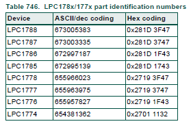
The part IDs didn't make much sense. Why not just give them the values of 1774 to 1788? Then I realized that they were flags that showed the capabilities of the processor. So I sat down with the various manuals and started decoding the flags. After about an hour, I ended up with a set of #defines that masked out bitfields or defined bits denoting the capabilities of the processor.
The part ID is read by calling into the NXP boot code at address 0x1FFF1FF1 using the In Application Programming (IAP) command 54. See the Flash Memory chapter in each processor user manual for more information on how to make the call. One thing not mentioned in the documentation is that you must disable interrupts because the exception vector table at address 0 may be remapped during the call.
NXP LPC17xx/40xx processor line comes in two families with four groups in each family. The processor families are LPC17xx and LPC40xx, and the groups are LPCxx5x, LPCxx6x, LPCxx7x, and LPCxx8x.
The following are the definitions I use to extract the various bit fields and flags. To extract a bit field, shift the part ID right by the shift value and then apply the mask. To check a bit, AND it with the part ID and check for nonzero.
#define Bit(BitNum)     (1u << (BitNum))

#define NXP_FAMILY_SHIFT        28      //!< Family right shift value
#define NXP_FAMILY_MASK         0x0Fu   //!< Family mask
#define NXP_FAMILY_LPC17xx      0x02u   //!< LPC17xx family
#define NXP_FAMILY_LPC40xx      0x04u   //!< LPC40xx family

#define NXP_GROUP_SHIFT         24      //!< Group right shift value
#define NXP_GROUP_MASK          0x0Fu   //!< Group mask
#define NXP_GROUP_LPCxx5x       0x05u   //!< LPCxx5x group
#define NXP_GROUP_LPCxx6x       0x06u   //!< LPCxx6x group
#define NXP_GROUP_LPCxx7x       0x07u   //!< LPCxx7x group
#define NXP_GROUP_LPCxx8x       0x08u   //!< LPCxx8x group

#define NXP_120_MHZ          (1u << 20) //!< 120 MHz capable
#define NXP_SD_CARD          (1u << 19) //!< SD card
#define NXP_LCD              (1u << 18) //!< LCD
#define NXP_PRAM             (1u << 16) //!< Peripheral memory (PRAM) available
#define NXP_PRAM_32K         (1u << 13) //!< 32K peripheral memory
#define NXP_CAN              (1u << 12) //!< CAN bus
#define NXP_ETHERNET         (1u << 11) //!< Ethernet
#define NXP_USB_OTG          (1u << 10) //!< USB On-The-Go
#define NXP_USB_HOST         (1u <<  9) //!< USB host
#define NXP_USB              (1u <<  8) //!< USB

#define NXP_RAM_SHIFT           4       //!< RAM size right shift value
#define NXP_RAM_MASK            0x0Fu   //!< RAM size mask
#define NXP_RAM_8K              0x01u   //!< 8 KB RAM
#define NXP_RAM_16K             0x02u   //!< 16 KB RAM
#define NXP_RAM_32K             0x03u   //!< 32 KB RAM
#define NXP_RAM_64K             0x04u   //!< 64 KB RAM

#define NXP_LPC1751_CRP      (1u <<  3) //!< CRP (LPC1751 only, else always 0)

#define NXP_FLASH_SHIFT         0       //!< Flash size right shift value
#define NXP_FLASH_MASK          0x07u   //!< Flash size mask
#define NXP_FLASH_32K           0x00u   //!< 32 KB flash
#define NXP_FLASH_64K           0x01u   //!< 64 KB flash
#define NXP_FLASH_128K          0x02u   //!< 128 KB flash
#define NXP_FLASH_256K          0x03u   //!< 256 KB flash
#define NXP_FLASH_512K          0x07u   //!< 512 KB flash


- Comments
- Write a Comment Select to add a comment

Hello
I am facing this issue with LPC1768-----> the RTC work fine only with mains power ON,even if coin battery of 3.3v connected to RTC pin. While initiating the program the backup registers need to be read to load the RTC value. But in my case after resetting the power the backup registers not storing the RTC value.
please suggest what is the solution...Thanks
Ajit

You should check the voltage on the VBAT pin with power off to the processor and make sure that you see 3.3v on the pin. If you don't see any voltage, the battery may be dead, or the battery circuit is bad.
Also make sure that you are writing 0 to the undefined RTC register bits. Some bits are used for testing and can cause the counters to all increment at the same time or not increment at all.
You also need a 32 KHz crystal connected to the RTCX1 and RTCX2 pins. Without it, the RTC won't count.
Here's my RTC init sequence:
1. Apply power to the RTC peripheral by writing a 1 to bit 9 (PCRTC) in the PCONP register
2. Write 0 to the Clock Control register (CCR)
3. Write 1 to the Enable bit (CLKEN) to enable the RTC
4. Write 1 to the Oscillator Fail bit (RTC_OSCF) in the Aux register (RTC_AUX) to clear the Oscillator Fail detect flag.
Thanks for your information, I will check with my design..
To post reply to a comment, click on the 'reply' button attached to each comment. To post a new comment (not a reply to a comment) check out the 'Write a Comment' tab at the top of the comments.
Please login (on the right) if you already have an account on this platform.
Otherwise, please use this form to register (free) an join one of the largest online community for Electrical/Embedded/DSP/FPGA/ML engineers:


