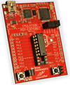
i have custome design for lpc2478 and flash SST39VF3202. Need to test the
interface with EMC controller. can anybody give me the test code.
Can anybody tell the Initialization of EMC of LPC2478?
lpc2478 and flash SST39VF3202
Started by ●September 9, 2011
Reply by ●September 9, 20112011-09-09
The init of the EMC also depends on how you connected the flash to the LPC. I
have only just started on the LPC2468 but this is what I did, not really sure
yet if it works correctly. I know that my SDRAM works, but still testing the
other (static memory) part.
The SDRAM part comes from application note AN10771.
void EMC_Init (void)
{
unsigned int i;
unsigned short wtemp;
//Pin Connect Block
// Assign pins to EMC controller(SDRAM )
PINSEL5&=0xF0FCFCC0;
PINSEL5|=0x05010115;
PINMODE5&=0xF0FCFCC0;
PINMODE5|=0x0A02022A;
//p2.29(DQMOUT1),28(DQMOUT0),24(CKEOUT0),20(DYCS0),18(CLKOUT0),17(RAS),16(CAS)
//p2.16,17,18,20,24,28,29 mode
//Pinmode (Pin has neither pull-up nor pull-down resistor enabled.)
PINSEL6 = 0x55555555;
PINMODE6 = 0xAAAAAAAA;
//p3.0-1515,mode
PINSEL8 &= 0xC0000000;
PINSEL8 |= 0x15555555;
PINMODE8&= 0xC0000000;
PINMODE8|= 0x2AAAAAAA;
//p4.0-4.14-14,mode
PINSEL9 &= 0x3FF0C3FF;
PINSEL9 |= 0x40051400;
PINMODE9&= 0x3FF0C3FF;
PINMODE9|= 0x800A2800;
//p4.31(CS1),25(WE),24(OE),22(A22),21(A21),MODE ,
// p4.31(CS1),24(OE),22(A22),21(A21) for nand flash
// Init SDRAM controller
// Enable EMC clock
PCONP|=0x800; //enable EMC power
EMC_CTRL=1; // enable EMC
EMC_DYN_RD_CFG=1;//Configures the dynamic memory read strategy(Command delayed strategy)
EMC_DYN_RASCAS0|=0x200;EMC_DYN_RASCAS0&=0xFFFFFEFF;//CAS latency=2
EMC_DYN_RASCAS0|=0x3; // RAS latency(active to read/write delay)=3
EMC_DYN_RP= P2C(SDRAM_TRP);
EMC_DYN_RAS = P2C(SDRAM_TRAS);
EMC_DYN_SREX = SDRAM_TXSR;
EMC_DYN_APR = SDRAM_TAPR;
EMC_DYN_DAL =SDRAM_TDAL ;
EMC_DYN_WR = SDRAM_TWR;
EMC_DYN_RC = P2C(SDRAM_TRC);
EMC_DYN_RFC = P2C(SDRAM_TRFC);
EMC_DYN_XSR = SDRAM_TXSR;
EMC_DYN_RRD = P2C(SDRAM_TRRD);
EMC_DYN_MRD = SDRAM_TMRD;
EMC_DYN_CFG0 = 0x0000680;
//16 bit external bus, 256 MB (16Mx16), 4 banks, row length = 13, column length = 9
// JEDEC General SDRAM Initialization Sequence
// DELAY to allow power and clocks to stabilize ~100 us
// NOP
EMC_DYN_CTRL = 0x0183;
//Issue SDRAM NOP (no operation) command ; CLKOUT runs continuously;All clock enables are driven HIGH continuously
for(i = 200*30; i;i--);
EMC_DYN_CTRL|=0x100; EMC_DYN_CTRL&=0xFFFFFF7F; //Issue SDRAM PALL (precharge all) command.
EMC_DYN_RFSH = 1; //Indicates 1X16 CCLKs between SDRAM refresh cycles.
for(i= 128; i; --i); // > 128 clk
EMC_DYN_RFSH = P2C(SDRAM_REFRESH) >> 4; // //Indicates ?? CCLKs between SDRAM refresh cycles.
EMC_DYN_CTRL|=0x80; EMC_DYN_CTRL&=0xFFFFFEFF; //Issue SDRAM MODE command.
wtemp = *((volatile unsigned short *)(SDRAM_CS0_BASE | 0x00023000)); /* 8 burst, 2 CAS latency */
EMC_DYN_CTRL = 0x0000; //Issue SDRAM norm command ; CLKOUT stop;All clock enables low
EMC_DYN_CFG0|=0x80000; //Buffer enabled for accesses to DCS0 chip
// And now for static
EMC_STA_CFG1 = 0;
EMC_STA_WAITWEN1 = 0x0F; // max time CS -> WRITE_ENABLE
EMC_STA_WAITOEN1 = 0x0F; // max time CS -> OUTPUT_ENABLE
EMC_STA_WAITRD1 = 0x1F; // time CS -> read access
EMC_STA_WAITPAGE1 = 0x1F; // time CS -> read access (page mode)
EMC_STA_WAITWR1 = 0x1F; // time CS -> write access
EMC_STA_WAITTURN1 = 0x0F; // time between read & write & static v. dynamic
}
--- In l..., "bhupesh" wrote:
>
> i have custome design for lpc2478 and flash SST39VF3202. Need to test the interface with EMC controller. can anybody give me the test code.
> Can anybody tell the Initialization of EMC of LPC2478?
>


