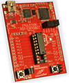
I have configured my LPC2148 to use both serial ports below the configuration:
void uart0_init(void)                //9600 BAUDIOS        pclock 48MHZ
{
 PCONP    |= 0x00000008;/* PCRTC = 1 */
 PINSEL0 |=0x00000005;            // Enable RxD0 and TxD0      AND Enable RxD1 and TxD1
 //U0FCR=0x07;                    //enable FIFO
 U0LCR=0X83;            //8-data bits, 1 Stop bit, Disable Parity and Enable DLAB
 U0DLL=0x38;                            //    MULVAL = 0x5 and DIVADDVAL = 14
 U0DLM=1;
 //U0FDR= 0x00000010;            //    MULVAL = 1 and DIVADDVAL = 0
 U0LCR=0X03;            //cleared DLAB
// U0IER= 0x00000001;
}
void uart1_init(void)                //9600 BAUDIOS        pclock 48MHZ
{
 //U0FCR=0x07;                    //enable FIFO
    PCONP |= 0x00000010;
 PINSEL0 |= 0x00050000; /* Enable RxD1 and TxD1*/
 U1LCR=0X83;            //8-data bits, 1 Stop bit, Disable Parity and Enable DLAB
 U1DLL=0x38;                            //    MULVAL = 0x5 and DIVADDVAL = 14
 U1DLM=1;
 //U0FDR= 0x00000010;            //    MULVAL = 1 and DIVADDVAL = 0
 U1LCR=0X03;            //cleared DLAB
 //U1IER= 0x00000001;
}
When I confirm in the simulation I can see the UART1 that can be transmitted correctly but when I charge it to the LPC it does not transmit or receive. I Check the physical connections in the micro and they are fine, in fact I change it for another one but the problem continues does not transmit or receive.
any suggestions?
#UART
I have looked over your configuration for PCONP and PINSEL and they appear to be correct. UART0 is also used by the boot loader for In System Programming(ISP), so I would look into the state of P0.14. If P0.14 is floating then you can get some odd behavior. If this is the case, I would really expect the MCU to not always execute the application, however it is worth a look. Here is the excerpt from the user manual.
"The flash boot loader code is executed every time the part is powered on or reset. The loader can execute the ISP command handler or the user application code. A a LOW level after reset at the P0.14 pin is considered as an external hardware request to start the ISP command handler. Assuming that proper signal is present on X1 pin when the rising edge on RESET pin is generated, it may take up to 3 ms before P0.14 is sampled and the decision on whether to continue with user code or ISP handler is made. If P0.14 is sampled low and the watchdog overflow flag is set, the external hardware request to start the ISP command handler is ignored. If there is no request for the ISP command handler execution (P0.14 is sampled HIGH after reset), a search is made for a valid user program. If a valid user program is found then the execution control is transferred to it. If a valid user program is not found, the auto-baud routine is invoked.Pin P0.14 that is used as hardware request for ISP requires special attention. Since P0.14 is in high impedance mode after reset, it is important that the user provides external hardware (a pull-up resistor or other device) to put the pin in a defined state. Otherwise unintended entry into ISP mode may occur."
1. Check the power, the state of the reset pin and as @hodgec pointed out, the state of the ISP pin.
2. If it's all good, check that your code is actually running. Forget the UARTS, just toggle a port pin in a never-ending loop. If you have the vector table checksum incorrectly set, the chip is stuck in ISP mode and your code is not running at all.
3. If the code is running, check that the pins are configured correctly. For starters, the TXD pin should be an output, idling high. If you can pull it down to GND with a 1k resistor, then your pin config is definitely not good.
4. If it all looks good, then you can start debugging by wiggling spare port pins at certain parts of the code and looking at the scope; welcome to bare metal firmware development :-) Unless, of course, you have a fancy debugger connected to the trace module of the chip, in which case just trace everything from reset.

If you are using 48 MHz clock, with 16 clocks for UART synchronisation, the effective clock rate would be: 48 MHz/ 16 = 3 MHz.
If this is used for generating baud rate of 9600, the divisor value should be: 3000000/9600 = 312.5
If you have supplied 312 as divisor it should be: 0x138, looks like correct value.
You confirm whether you have used any value to divide the 48 MHz clock when you are supplying to the peripheral.


