


How FPGAs work, and why you'll buy one
Today, pretty much everyone has a CPU, a DSP and a GPU, buried somewhere in their PC, phone, car, etc. Most don't know or care that they bought any of these, but they did.
Will everyone, at some future point, also buy an FPGA? The market size of FPGAs today is about 1% of the annual global semiconductor sales (~$3B vs ~$300B). Will FPGA eventually become a must-have, or will its volume remain relatively low?
We'll try to answer this question below. In order to see how popular FPGAs could become, we'll need to discuss what FPGAs are. FPGAs are a programmable platform, but one designed by EEs for EEs rather than for programmers. So for many programmers, FPGAs are exciting yet mysterious; I hope our discussion will help demystify them.
We'll start with a common explanation of FPGAs' relatively low popularity. We'll see why that explanation is wrong - and why, if we take a closer look, we actually come to expect FPGAs to blow the competition out of the water!
This will conclude today's installment, "Why you'll buy an FPGA". A sequel is in the making, titled "Why you won't buy an FPGA". There, we'll see some of the major obstacles standing between FPGAs and world domination.
The oft-repeated wrong answer
…to the question of "why aren't FPGAs more popular?" is, "FPGA is a poor man's alternative to making chips. You can implement any circuit design in an FPGA, but less efficiently than you could in an ASIC or a custom design. So it's great for prototyping, and for low-volume products where you can't afford to make your own chips. But it makes no sense for the highest-volume devices - which happen to add up to 99% of sales, leaving 1% to FPGAs."
This is wrong because programmability is a feature, not just a tax on efficiency.
Of course a Verilog program doing convolution on an FPGA would run faster if you made a chip that runs just that program. But you typically don't want to do this, even for the highest-volume products, any more than you want to convert your C programs running on CPUs into dedicated hardware! Because you want to change your code, run other programs, etc. etc.
When programmability is required - which is extremely often - then the right thing to compare FPGAs to is another programmable platform: a DSP, a GPU, etc. And, just like FPGAs, all of these necessarily introduce some overhead for programmability. So we can no longer assume, a priori, that any one option is more efficient than another - as we did when comparing FPGAs to single-purpose ASICs.
We need benchmarks - and FPGAs' performance appears very competitive in some benchmarks. Here's what BDTI's report from 2007 says:
…we estimated that high-end FPGAs implementing demanding DSP applications … consume on the order of 10 watts, while high-end DSPs consume roughly 2-3 watts. Our benchmark results have shown that high-end FPGAs can support roughly 10 to 100 times more channels on this benchmark than high-end DSPs…
So for that benchmark, FPGAs offer 10x-100x the runtime performance, and 2x-30x the energy efficiency of DSPs - quite impressive!
But wait - how are they so efficient?
FPGAs are no longer FPGAs
Aren't FPGAs Field-Programmable Gate Arrays?
Programmable gate arrays can't multiply as efficiently as dedicated multipliers, can they? A dedicated multiplier is a bunch of gates connected with wires - the specific gates that you need for multiplying, connected specifically to the right other gates as required for multiplication.
A programmable gate array is when your gates are generic. They index into a truth table (called a look-up table or LUT) with their inputs, and fetch the answer. With a 2-input LUT, you get an OR gate or an AND gate or whatever, depending on the truth table you programmed. With 3-input LUTs, you can have a single gate computing, say, (a&b)|c, but the principle is the same:
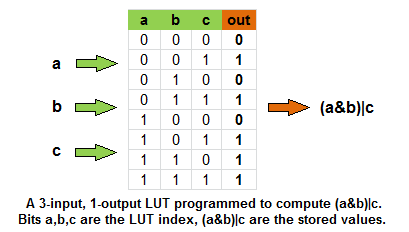
This absolutely must be bigger and slower than just an OR gate or an AND gate!
Likewise, wires go through programmable switch boxes, which connect wires as instructed by programmable bits:
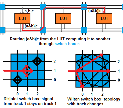
There are several switch box topologies determining which wires can be connected to which. But whatever the topology, this must be bigger and slower than wires going directly to the right gates.
All this is indeed true, and a "bare" FPGA having nothing but programmable gates and routers cannot compete with a DSP. However, today's FPGAs come with DSP slices - specialized hardware blocks placed amidst the gates and routers, which do things like multiply-accumulate in "hard", dedicated gates.
So that's how FPGAs compete with DSPs - they have DSP hardware in them! Cheating, isn't it?
Well, yes and no.
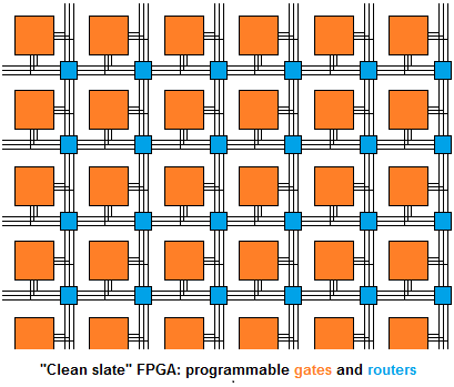
It's "cheating" in the sense that FPGAs aren't really FPGAs any more - instead, they're arrays of programmable gates plus all that other stuff. A "true FPGA" would look like this:
Instead, a high-end modern FPGA looks like this:
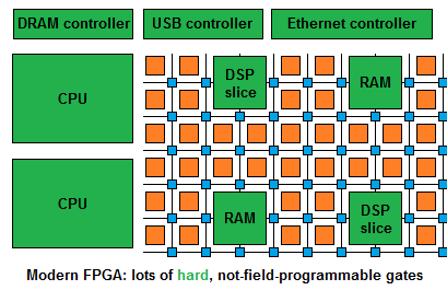
To be competitive in DSP applications, FPGAs need DSP slices - ALUs doing things like multiply-accumulates.
To be competitive in applications needing a CPU - which is most of them - today's FPGAs have more than just specialized ALUs. They have full-blown ARM cores implemented using "hard", non-programmable gates!
So you've been "cheated" if you thought of FPGAs as "clean slates" suitable for any design. In reality, FPGAs have specialized hardware to make them competitive in specific areas.
And you can sometimes guess where they're less competitive by observing which specializations they lack. For instance, there are no "GPU slices", and indeed I don't believe FPGAs can compete with GPUs in their own domain as they compete with DSPs. (Why not simply add GPU slices then? Here the plot thickens, as we'll see in the follow-up article.)
But of course having DSP slices is more than just "cheating" - because look at just how many DSP slices FPGAs have. The cheapest FPGAs can do hundreds of mutliply-accumulates simultaneously! (My drawing above has the wrong scale - imagine hundreds of small DSP slices near a couple of much larger CPUs.)
And hundreds of MACs is a big deal, because while anyone can cram a load of multipliers into a chip, the hard part is to connect it all together, letting a meaningful program actually use these multipliers in parallel.
For instance, TI's C64 DSPs can do 8 MACs per cycle - but only if it's a dot product. TI's C66 DSPs can do 32 MACs/cycle - but only if you're multiplying complex numbers. You only get the highest throughput for very specific data flows.
To the extent that the FPGA architecture lets you actually use an order of magnitude more resources at a time, and do that in more real-life examples, it is a rather unique achievement. And this is how they actually beat dedicated DSPs with their DSP slices, not just reach the same performance.
FPGA as a programmable accelerator architecture
So what makes FPGAs such an efficient architecture? There's no simple answer, but here are some things that FPGAs can use to their advantage:
- No need for full-blown ALUs for simple operations: a 2-bit adder doesn't need to be mapped to a large, "hard" DSP slice - it can fit comfortably in a small piece of "soft" logic. With most processors, you'd "burn" a full-blown ALU to do the simplest thing.
- No need for a full cycle for simple operations: on FPGAs, you don't have to sacrifice a full cycle to do a simple operation, like an OR, which has a delay much shorter than a full cycle. Instead, you can feed OR's output immediately to the next operation, say, AND, without going through registers. You can chain quite a few of these, as long as their delays add up to less than a cycle. With most processors, you'd end up "burning" a full cycle on each of these operations.
- Distributed operand routing: most processors have their ALUs communicate through register files. With all the ALUs connected to all the registers, there's a bottleneck - this interconnect grows as the product of the number of ALUs and registers, so you can't have too many of either. FPGAs spread ALUs and registers throughout the chip, and you can connect them in ways not creating such bottlenecks - say, as a long chain, as a tree, and in many other ways. Of course you can also route everything through a bottleneck, and then your design will run at a low frequency - but you don't have to. With CPUs or DSPs, they run at a high frequency - because the amount of ALUs and registers was limited to make that frequency possible. But in FPGAs you can get both high frequencies and a lot of resources used in parallel.
- Distributed command dispatching: a 2-issue or a 6-issue processor is common, but 100-issue processors are virtually unheard of. Partly it's because of the above-mentioned operand routing, and partly it's because of command dispatching - you'd have to fetch all those commands from memory, another bottleneck. In FPGAs, you can implement command-generating logic in simple state machines residing near your ALUs - and in the simplest case, commands are constants kept in registers residing near ALUs. This lets you easily issue 100 parallel instructions.
This "distributed" business is easier to appreciate by looking at an example. Here's a schematic implementation of a 1D convolution on an FPGA - you convolve a long vector v with an N-coefficient filter f, computing, at every i, f0*v[i] + f1*v[i-1] + f2*v[i-2] + … + fN-1*v[i-N-1]:
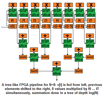
In this drawing, N=8, but it scales easily to arbitrary N, producing results at a slightly larger latency - the summation tree depth being log(N).
The orange boxes are registers; commands like + and * are stored in registers, as are inputs and outputs. (I'm feeding the output of * to + directly without going through a register to save screen space.) Every clock cycle, inputs are fed to ALUs, and the outputs become the new register values.
Orange boxes (registers) spread amongst green boxes (ALUs) illustrate "distributed operand and command routing". If you wonder how it all looks like in code, Verilog source code corresponding to this drawing appears near the end of the article.
And here's a linear pipeline without a summation tree:
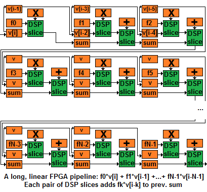
This is a little trickier, at least to me (I had a bug in my first drawing, hopefully it's fixed). The idea is, every pair of ALUs computes a product of fk with v[i-k], adds it to the partial sum accumulated thus far, and sends the updated partial sum downstream to the next pair of ALUs.
The trick is this. The elements of v are also moving downstream, together with the sums. But after v[i] got multiplied by f0, you don't want to multiply it by f1 in the next cycle. Instead, you want to multiply v[i-1] by f1 - that's the product that we need for the convolution at index i. And then you do want to multiply v[i] by f1 once cycle later - for the convolution at index i+1. I hope that my sampling of v[i] to an intermediate register, which delays its downstream motion, does the trick.
So these two examples show how FPGA programming is different from programming most kinds of processors - and how it can be more efficient. More efficient, because you can use a lot of ALUs simultaneously with little overhead spent on dispatching commands and moving inputs and outputs between ALUs. An argument can be made that:
- FPGAs are more flexible than SIMD/SIMT. You can give different instructions to different ALUs, and you can route operands from different places. Contrast this with SIMD instructions like add_16_bytes, with byte i always coming from offset i inside a wide register.
- FPGAs scale better than VLIW/superscalar. More instructions can be issued simultaneously, because there's no routing bottleneck near the register file, and no instruction memory bandwidth bottleneck.
- FPGAs are more efficient than multiple cores. Multiple cores are flexible and can scale well. But you pay much more overhead per ALU. Each core would come with its own register files and memories, and then there are communication overheads.
This gives us a new perspective on LUTs and switch boxes. Yes, they can be an inefficient, cheaper-to-manufacture alternative to dedicated gates and wires. But they are also a mechanism for utilizing the "hard" components spread in between them - sometimes better than any other mechanism.
And this is how FPGAs beating DSPs with the help of DSP slices isn't "cheating". (In fact, mature DSPs "cheat" much more by having ugly, specialized instructions. Far more specialized than FPGAs' multiply-accumulate, dot product instructions being among the least ugly. And the reason they need such instructions is they don't have the flexibility of FPGAs, so what FPGAs effectively do in software, they must do in hardware in order to optimize very specific data flows.)
I/O applications
But wait - there's more! In addition to being a hardware prototyping platform and an accelerator architecture, FPGAs are also uniquely suited for software-defined I/O.
"Software-defined I/O" is the opposite of "hardware-defined I/O" - the common state of things, where you have, for instance, an Ethernet controller implementing some share of TCP or UDP in hardware. Software-defined I/O is when you have some programmable hardware instead of dedicated hardware, and you implement the protocols in software.
What makes FPGAs good at software-defined I/O?
- Timing control: Verilog and other hardware description languages give you more precise control over timing than perhaps any other language. If you program it to take 4 cycles, it takes 4 cycles - no cache misses or interrupts or whatever will get in your way unexpectedly. And you can do a whole lot in these 4 cycles - FPGAs are good at issuing plenty of instructions in parallel as we've seen. This means you don't have to account for runtime variability by buffering incoming data, etc. - you know that every 4 cycles, you get a new byte/pixel/etc., and in 4 cycles, you're done with it. This is particularly valuable where "deep" buffering is unacceptable because the latency it introduces is intolerable - say, in a DRAM controller. You can also do things like generating a clock signal at a desired frequency, or deal with incoming clock signal at a different frequency than yours.
- Fine-grained resource allocation: you "burn" a share of FPGA resources to handle some peripheral device - and that's what you've spent. With other processor cores, you'll burn an entire core - "this DSP handles WiFi" - even if the core is idle much of the time. (The FPGA resources are also burnt that way - but you'll often spend less resources than a full processor core takes.) Alternatively, you can time-share that DSP core - but it's often gnarly. Many kinds of cores expose a lot of resources that must be manually context-switched at an intolerably high latency. Core asymmetry gets in the way of thread migration. And with two I/O tasks, often none can tolerate being suspended for a long while, so you'll definitely burn two cores. (One solution is hardware multithreading.)
The upshot is that relatively few processors other than FPGAs are suitable for software-defined I/O. The heavily multi-threaded XMOS is claimed to be one exception. Then there are communication processors such as the hardware-threaded Qualcomm Hexagon DSP and the CEVA-XC DSPs. But these are fairly specialized; you couldn't use them to implement a memory controller or an LVDS-to-parallel video bridge, both of which you could do with an FPGA.
And of course, FPGA's I/O capabilities can be combined with computation acceleration - get pixels and enhance the image color on the fly, get IP packets with stock info and decide which stocks to trade on the fly.
Programmable, efficient, and versatile, FPGAs are starting to sound like a great delivery platform.
Summary
There are several points that I tried to make. Some are well-known truisms, and others are my own way of looking at things, which others might find debatable or at least unusually put.
- While FPGA are a great small-scale circuit delivery platform, they can also be a large-scale software delivery platform. You can think of FPGAs as "inefficiently simulating circuits". But in other contexts, you can also think of them as "efficiently executing programs"!
- Instead of fixed-function gates and wires connecting specific gates to each other, FPGAs use programmable gates - configured by setting a truth table of choice - and programmable switch boxes, where incoming wires are connected to some of the other wires based on configuration bits. By itself, it's very inefficient compared to a "direct" implementation of a circuit.
- Then how can FPGAs beat, not just CPUs, but specialized accelerators like DSPs in their own game? The trick is, they're no longer FPGAs - gate arrays. Instead, they're also arrays of RAMs and DSP slices. And then they have full-blown CPUs, Ethernet controllers, etc. implemented in fixed-function hardware, just like any other chip.
- In such modern FPGAs, the sea of LUTs and switch boxes can be used not instead of fixed-function circuits, but as a force multiplier letting you make full use of your fixed-function circuits. LUTs and switch boxes give two things no other processor architecture has. First, the ability to use less than a full-blown ALU for simple things - and less than a full clock cycle. Second, distributed routing of commands and operands - arguably more flexible than SIMD, more scalable than superscalar execution, and more efficient than multiple instruction streams.
- FPGAs are the ultimate platform for software-defined I/O because of their timing control (if I said 4 cycles, it takes 4 cycles) and fine-grained resource allocation (spend so many registers and ALUs per asynchronous task instead of dedicating a full core or having to time-share it).
With all these advantages, why just 1% of the global semiconductor sales? One reasonable answer is that it took FPGAs a long time to evolve into their current state. Things FPGAs have today that they didn't have in the past include:
- Fixed-function hardware essential for performance - this gradually progressed from RAM to DSP slices to complete CPUs.
- Quick runtime reconfiguration, so that you can run convolution and then replace it with FFT - which you can't, and shouldn't be able to do, if you're thinking of FPGA as simulating one circuit.
- Practically useable C-to-Verilog compilers, letting programmers, at least reasonably hardcore ones, who nonetheless aren't circuit designers, to approach FPGA programming easily enough.
All of these things cater to programmers as much or more than they cater to circuit designers. This shows that FPGAs are gunning for a position in the large-scale software delivery market, outside their traditional small-scale circuit implementation niche. (Marketing material by FPGA vendors confirms their intentions more directly.)
So from this angle, FPGAs evolved from a circuit implementation platform into a software delivery platform. Being a strong programmable architecture, they're expected to rise greatly in popularity, and, like other programmable architectures, end up everywhere.
Unanswered questions
As a teaser for the sequel, I'll conclude with some questions which our discussion left unanswered.
Why do FPGAs have DSP slices and full-blown "hard" CPUs? Why not the other way around - full-blown DSP cores, and some sort of smaller "CPU slices"? Where are the GPU slices? And if rationing individual gates, flip-flops and picoseconds instead of full ALUs, registers and clock cycles is so great, why doesn't everyone else do it? Why do they all break up resources into those larger chunks and only give software control over that?
Stay tuned for the sequel - "How FPGAs work, and why you won't buy one".
P.S. Programmable - how?
So how do you program the programmable gate array? Talk is cheap, and so are Microsoft Paint drawings. Show me the code!
The native programming interface is a hardware description language like Verilog. Here's an implementation of the tree-like convolution pipeline in Verilog - first the drawing and then the code:
module conv8(clk, in_v, out_conv);
  //inputs & outputs:
  input clk; //clock
  input [7:0] in_v; //1 8-bit vector element
  output reg [18:0] out_conv; //1 19-bit result

  //internal state:
  reg [7:0] f[0:7]; //8 8-bit coefficients
  reg [7:0] v[0:7]; //8 8-bit vector elements
  reg [15:0] prod[0:7]; //8 16-bit products
  reg [16:0] sum0[0:3]; //4 17-bit level 0 sums
  reg [17:0] sum1[0:1]; //2 18-bit level 1 sums

  integer i; //index for loops unrolled at compile time

  always @(posedge clk) begin //when clk goes from 0 to 1
    v[0] <= in_v;
    for(i=1; i<8; i=i+1)
      v[i] <= v[i-1];
    for(i=0; i<8; i=i+1)
      prod[i] <= f[i] * v[i];
    for(i=0; i<4; i=i+1)
      sum0[i] <= prod[i*2] + prod[i*2+1];
    for(i=0; i<2; i=i+1)
      sum1[i] <= sum0[i*2] + sum0[i*2+1];
    out_conv <= sum1[0] + sum1[1];
  end
endmodule
This example shows how "distributed routing" actually looks in code - and the fine-grained control over resources, defining things like 17-bit registers.
And it's fairly readable, isn't it? Definitely prettier than a SIMD program spelled with intrinsics - and more portable (you can target FPGAs by different vendors as well as an ASIC implementation using the same source code; it's not trivial, but not hopeless unlike with SIMD intrinsics, and probably not harder than writing actually portable OpenCL kernels.)
Incidentally, Verilog is perhaps the quintessential object-oriented language - everything is an object, as in a physical object: a register, a wire, a gate, or a collection of simpler objects. A module is like a class, except you can't create objects (called instantiations) dynamically - all objects are known at compile time and mapped to physical resources.
Verilog insists on encapsulation as strictly as it possibly could: there's simply no way to set an object's internal state. Because how could you affect that state, physically, without a wire going in? Actually, there is a way to do that - the usual instance.member syntax; hardware hackers call this "an antenna", because it's "wireless" communication with the object's innards. But it doesn't synthesize - that is, you can do it in a simulation, but not in an actual circuit.
Which means that our example module is busted, because we can't initialize the filter coefficients, f. In simulations, we can use antennas. But on an FPGA, we'd need to add, say, an init_f input, and then when it's set to 1, we could read the coefficients from the same port we normally use to read v's elements. (BTW, not that it adds much efficiency here, but the "if" test below is an example of an operation taking less than a cycle.)
always @(posedge clk) begin
  if(init_f) begin
    f[0] <= in_v;
    for(i=1; i<8; i=i+1)
      f[i] <= f[i-1];
  end
end
A triumph of encapsulation, it's also a bit of a pity, because there are now actual wires and some control logic sitting near our coefficient registers, enlarging the circuit, only to be used upon initialization. We're used to class constructors "burning" a few memory bits; who cares - the bits are quickly swapped out from the instruction cache, so you haven't wasted resources of your computational core. But Verilog module initialization "burns" LUTs and wires, and it's not nearly as easy to reuse them for something else. We'll elaborate on this point in the upcoming sequel.
Not only is Verilog object-oriented, but it's also the quintessential language for event-driven programming: things are either entirely static (these here bits go into this OR gate), or triggered by events (changes of signals, very commonly a clock signal which oscillates between 0 and 1 at some frequency). "always @(event-list)" is how you say what events should cause your statements to execute.
Finally, Verilog is a parallel language. The "static" processes, like bits going into OR gates, as well as "event-driven processes", like statements executing when the clock goes from 0 to 1, all happen in parallel. Within a list of statements, "A <= B; C <= A;" are non-blocking assignments. They happen in parallel, so that A is assigned the value of B, and C is simultaneously assigned the (old) value of A.
So, for example, prod[i]<=f[i]*v[i] sets the new value of prod, and in parallel, sums are computed from the old values of prod, making it a pipeline and not a serial computation. (Alternatively, we could use blocking assignments, "=" instead of "<=", to do it all serially. But then it would take more time to execute our series of statements, lowering our frequency, as clk couldn't switch from 0 to 1 again until the whole serial thing completes. Synthesis tools tell you the maximal frequency of your design when they're done compiling it.)
On top of its object-oriented, event-based, parallel core, Verilog delivers a ton of sweet, sweet syntactic sugar. You can write + and * instead of having to instantiate modules with "adder myadd(a,b)" or "multiplier mymul(a,b)" - though + and * are ultimately compiled down to module instances (on FPGAs, these are often DSP slice instances). You can use if statements and array indexing operators instead of instantiating multiplexors. And you can write loops to be unrolled by the compiler, generate instantiations using loop syntax, parameterize your designs so that constants can be configured by whoever instantiates them, etc. etc.
If all this doesn't excite you and you'd rather program in C, you can, sort of. There's been loads of "high-level synthesis tools" - basically C to Verilog compilers - and their quality increased over the years.
You'd be using a weird C dialect - no function pointers or recursion, extensions to specify the exact number of bits in your integers, etc. You'd have to use various #pragmas to guide the compilation process. And you'd have things like array[index++] not actually working with a memory array - and index++ not actually doing anything - because you're getting values, not from memory, but from a FIFO, or directly from the output of another module (just like in_v in our Verilog code doesn't have to come from memory, and out_conv doesn't have to go to memory.)
But you can use C, sort of - or Verilog, for real. Either way, you can write fairly readable FPGA programs.


- Comments
- Write a Comment Select to add a comment

I am agree with you,regarding the vendors software design like the IDE and the licenses for access to IP cores sometimes can be such a pain. There are some free projects over there, in specifically i am following a good one the name is Tinyfpga.com. Them have launched a low cost FPGA board.
Cheers!

Thank you for an excellent write-up on FPGAs.
I have limited exposure to these and found your article very useful.
Thank you, Have a beer!
My only experience with FPGA's was in college where we programmed in VHDL using Quartus. This article was an exciting look at new FPGA layouts (didn't know they technically cheated with self-contained DSPs!) as well as my first time seeing Verilog. Looking forward to reading the rest of the series! Thank you so much.
Excellent treatment !
I love FPGAs. and big ones. But I would say, if you can do it on a mcirocontroller or DSP, then do it, because the fpga will take you much longer. FPGA's come into it if you cannot do it on a micro and have enough in hand to tackle future hardware requirements,. Also they are good at dealing with specific interfaces, because whatever the interface is, the FPGA can handle it, and you would be stuck in whatever the peripherial does in the micro. and micro peripherals have bugs/ odd behaviour, which you can always fix in a FPGA.
DSPs and micros no longer have the power advantage either. FPGAs can run same or less power....
glen.
Xilinx user.
Great article!
To post reply to a comment, click on the 'reply' button attached to each comment. To post a new comment (not a reply to a comment) check out the 'Write a Comment' tab at the top of the comments.
Please login (on the right) if you already have an account on this platform.
Otherwise, please use this form to register (free) an join one of the largest online community for Electrical/Embedded/DSP/FPGA/ML engineers:


