VHDL tutorial
When I was first introduced to "Programmable Logic" several years ago, it was an answer to many of the challenges that I was struggling with. Though the parts were primitive by today's standards (simple PALs verses FPGA), they were an extremely cost effective tool addressing the need for specialized logic blocks.
Quick Links
- Part 1: VHDL tutorial
- Part 2: part 2 - Testbench
- Part 3: combining clocked and sequential logic
- Part 4: Creating a hierarchical design
- Part 5: A practical example - part 1 - Hardware
- Part 6: A practical example - part 2 - VHDL coding
- Part 7: A practical example - part 3 - VHDL testbench
I have continued to incorporate these powerful blocks into many of my latest designs. My current favorite part line is the Xilinx CoolRunner series (XC2Cxxx). In this article I will present a cut-down sample of one of my active design projects targeted for a XC2C32A CPLD.
This example is extracted from a recent data acquisition project. For this design, I had a need to generate a clock signal (ADCClk), that was to be programmable over a series of fixed rates (20MHz, 10MHz, 4MHz, 2MHz, 1MHz and 400KHz). The master clock for the device is fixed at 40MHz. The part has a simple 4-bit port (inByte), with a selectable register address (RegSel is used to select up to four registers, but for simplicity, only a single register address is shown). The addressed register is updated on the positive going edge of the register strobe signal (RegStrb). The clock rate is set through this port, at RegSel = "01", according to the table below. There is also a global reset line (SeqReset) that is used to preset the device to a known state when driven with a logic low.
| InByte @ RegSel = "01" | ADCClk rate |
| 000 | 20MHz |
| 001 | 10MHz |
| 010 | 4MHz |
| 011 | 2MHz |
| 100 | 1MHz |
| 101 to 111 | 400KHz |
To construct a VHDL module the first step is to define all of the inputs and outputs to the device. The following is the declaration of the inputs and outputs of the ClkDiv example. In the Xilinx ISE environment, the VHDL editor uses "--" as a comment line. In my code, I extend this comment construct to show the direction of my inputs/outputs (---- output) and the device that the part connects to. "STD_LOGIC" is a simple logic value, or bit, ('1', '0', 'X' or 'Z') while "STD_LOGIC_VECTOR" is used to define a bus, or word, made up of several bits.

The next step is to declare any signals (or variables) that are used inside of the design. In this example, I needed a single counter to represent the programmable count-down timer that will generate the clock signal (ADC_div). The counter needs to count through a range of 1 to 40, and is defined as 6-bit vector (STD_LOGIC_VECTOR(5 downto 0)). Additional signals are needed to create the 'toggle' register for the clock (ADDClk) and a register to hold the commanded clock rate (ClkSel). As the signals are created, the initial condition can be defined for the signals (":=" is used to specify the initial values).
![]()
With all the inputs, outputs and internal signals defined, we can start the fun part. The behavior of the part is then defined in a series of processes and assignments. Processes are executed when changes occur in the signals in the process's sensitivity list. Assignments are evaluated whenever signals of the right-hand side of the assignment statement change. In this example there are two processes and a single assignment.
The processes used in this example are to perform the clock division and to provide a simple, addressable latch to store the clock divisor command. The first process (ClkDiv) is executed whenever any of its inputs (Mclk or SeqReset) are changed. The input SeqReset is used to set all of the signals associated with this process to their default or initial conditions. This includes setting the initial value of the clock toggle (ADCClk) to '0'.
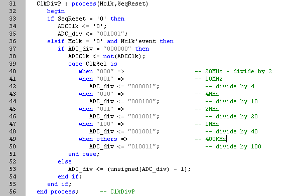
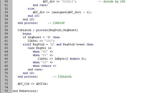
In the above figure, lines 33 to 35 are used to provide the reset condition. When SeqReset is set to '0' the signals (ADCClk and ADC_div) are set to their initial conditions. If the SegReset is not '0', the Mclk signal is tested for a falling edge (line 36 looks for change in Mclk with the current value of Mclk = '0'). If the condition is true, the rest of the logic is processed. The next test is a zero check of the ADC_div counter. If the counter is equal to "000000" (line 37), the ADCClk signal is toggled (line 38), i.e. if it is '0' it is set to '1' and vice versa. The next step is to reload the counter. The reload valve of the timer is determined by the ClkSel value. In VHDL, the case/when statements are used to take an action based on the current value of signal. In this example (lines 39 through 51) a case/when structure is used to handle the reload of the counter (ADC_div). If the counter (ADC_div) was not zero (line37), then the 'else' clause is executed and the ADC_div is decremented (line 53). In order to decrement the counter, the value is first cast to an unsigned value, then 1 is subtracted from the value. ADC_div is then updated with the new value.
The second process (ClkLatch) is executed whenever any of its inputs (RegStrb or SeqReset) are changed. The input SeqReset is used to set all of the signals associated with this process to their default or initial conditions. This includes setting the initial value of the clock select register (ClkSel) to "100" (divide by 40, or 1MHz).
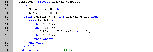
In the above figure, lines 60 to 61 are used to provide the reset condition. When SeqReset is set to '0' the signal (ClkSel) is set to its initial condition. If the SegReset is not '0', the RegStrb signal is tested for a rising edge (line 62 looks for change in RegStrb with the current value of RegStrb = '1'). If the condition is true, the case/when logic (lines 63 to 69) is processed. In this example only the clock select register is implemented. If RegSel signal is set to "01", the last three bits of the input signal (InByte) are transfered to the Clock select register (ClkReg).
The final step of the example is the assignment statement that transfers the internal signal (ADCClk) to the output pin (ADC_Clk). A separate, internal signal (ADCClk) is used, since the ClkDiv logic uses ADCClk as both an input and output ( ADCClk
![]()
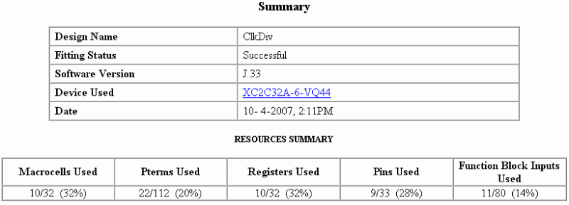
Putting all the pieces together we get a VHDL program for a Xilinx CPLD that is a programmable clock divider. The example, shown at the end of this article, compiled easily into the XC2C32A-6VQ44 part. The summary shows that the part is only partially full, leaving room for future enhancements.
In a future article, I will show some more advanced programs and a VHDL test bench to exercise the examples.
Happy designing!
Gene
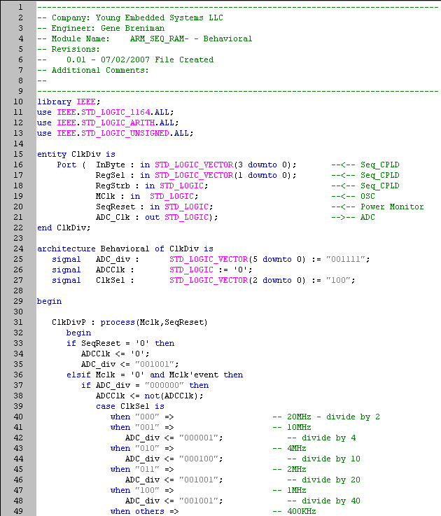
--------- Completed example -------
- Comments
- Write a Comment Select to add a comment

Hi Gene,
Can you please update your VHDL tutorial to use Numeric_std instead of std_logic_arith. Numeric_std is an IEEE standard that is being maintained. Std_logic_arith is open source software that was erroneously put in the IEEE library by EDA vendors.
Thanks,
Jim Lewis
IEEE 1076 Working Group Chair.

A classic article series. Thank you for your time and work.
To post reply to a comment, click on the 'reply' button attached to each comment. To post a new comment (not a reply to a comment) check out the 'Write a Comment' tab at the top of the comments.
Please login (on the right) if you already have an account on this platform.
Otherwise, please use this form to register (free) an join one of the largest online community for Electrical/Embedded/DSP/FPGA/ML engineers:


