


Voltage Drops Are Falling on My Head: Operating Points, Linearization, Temperature Coefficients, and Thermal Runaway
Today’s topic was originally going to be called “Small Changes Caused by Various Things”, because I couldn’t think of a better title. Then I changed the title. This one’s not much better, though. Sorry.
What I had in mind was the Shockley diode equation and some other vaguely related subjects.
My Teachers Lied to Me
My introductory circuits class in college included a section about diodes and transistors.
The ideal diode equation is this:
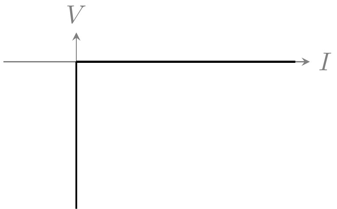
$$\begin{array}{} V = 0 & \text{if } I > 0 \cr I = 0 & \text{if } V < 0 \end{array} $$
In other words, a diode acts like a short circuit with positive current, to prevent any voltage drop, and it acts like an open circuit with negative voltage, to prevent any current flow.
But that’s not realistic.
So the next best thing is that we just assume there’s a diode drop of 0.7V or so:
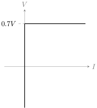
$$ \begin{array}{} V = 0.7 & \text{if } I > 0 \cr I = 0 & \text{if } V < 0.7 \end{array} $$
But that’s not much better.
So then we learned that the p-n junction equation, which applies to things like diodes and npn transistors and solar cells, has an exponential relationship:
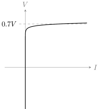
$$ V = \frac{kT}{q} \ln \frac{I}{I_s} $$
where \( k \) is Boltzmann’s constant (\( k \approx 1.380 \times 10^{-23} J/K \)), \( T \) is the temperature in degrees Kelvin, \( q \) is the charge of an electron (\( q \approx 1.602 \times 10^{-19} C \)), and \( I_s \) is some characteristic current of the junction in question. What’s “characteristic” here is really the current density, so for diodes and transistors \( I_s \) increases linearly with the area of the junction. Double the area and you double \( I_s \). At 25°C, \( \frac{kT}{q} \approx 25.7 \)mV, so when you hear “26 millivolts” batted around a lot in semiconductor theory, that’s where it comes from.
And actually, that’s not quite true either; in reality there’s a “+1” in the equation:
$$ V = \frac{kT}{q} \ln \left(\frac{I}{I_s} + 1\right) $$
But for all practical purposes you can forget about the “+1”, since for real devices, \( I_s \) tends to be in the sub-picoampere range.
So we’re left with \( V = \frac{kT}{q} \ln I/I_s \): at room temperature, double the current, and you increase the junction voltage by about 18 millivolts; increase the current by a factor of 10, and you increase the junction voltage by about 59 millivolts.
Great. That’s more or less what I’ve been using in my mental model of diodes and bipolar transistors for the last 20 years. This gives you the equation for \( V_{BE} \) in terms of base current, or if you fold the gain β into \( I_s \), in terms of collector current.
Except that’s not true either. My teachers lied to me! In doing research for this article, I found they left out a factor of n (or η if you like Greek letters):
$$ V = \frac{nkT}{q} \ln \left(\frac{I}{I_s} + 1\right) $$
This factor \( n \) is called the ideality factor, and it’s apparently between 1 and 2 for most devices. (Though if you’ve got your head in the sand, and don’t want to consider devices that have areas of operation with \( n > 1 \), then by definition \( n \approx 1 \) and everything is hunky-dory.)
And that’s not true either, because there are parasitic series resistances and other odd effects, which you learn about in more advanced areas of study.
It’s not unusual for teachers to lie to you. They have to! Everything we use in scientific modeling is an approximation; reality has all these ugly factors that would give you information overload and send you running away, if you heard about them all at once. For example, we think of dice as cubes, but really they have the edges and corners rounded off, with little indentations for the pips, and the surfaces aren’t perfectly parallel or perfectly smooth due to manufacturing limitations, and anyway you have quantum physics coming into the mix telling you that the atoms are moving around unpredictably, doing whatever funny stuff they do in quantumland.
So if you want to know more about why p-n junctions work the way they do, you take courses on device physics, whereas if you just want things to get done accurately, you deal with these effects empirically, like measure the ideality factor (Microchip has a good appnote on usage of diode-connected transistors; many of the commercially-available 2N3904 transistors, if used in a diode-connected manner, have ideality factors around the 1.004-1.005 range) and just deal with it. For the rest of us, just forget about \( n \) and pretend it’s equal to 1.
But that’s not what this article is about.
Small-Signal Analysis: Operating Points and Linearization
So let’s say that you have an electrical circuit put together, and all the currents and voltages are constant, and everything’s happy. You measure it and diligently figure out what all those currents and voltages are. That’s called an operating point.
Now you change one of the input currents or voltages, and add a really small signal \( x(t) \) to it, and measure one of the other signals \( y(t) \) and see how it relates to \( x(t) \). This is called small-signal analysis, and it generally relies on the assumption that for small changes in any of the variables or parameters, systems are linear in a small region around any particular operating point. It’s the same technique used to define derivatives: it’s just the limit of the ratio of one variable to another when deviations are small. This idea is also called linearization: for some vector of inputs \( X \) and vector of outputs \( Y \) around any given operating point \( (X_0, Y_0) \), we can approximate the outputs by \( Y \approx Y_0 + J(X_0, Y_0) \times (X - X_0) \) and J is the Jacobian, which is just a big matrix of partial derivatives \( J_{ij} = \partial y_i / \partial x_j \) . Blah blah blah. It’s hard to look at this abstract stuff and see what’s going on, so let’s look at a more concrete and useful example.
Let’s say that we have a diode with a 0.70V drop when it conducts 1 mA from a current source. In parallel with the diode is a 1μF capacitor, and we give the capacitor a little whack by discharging it from, say, 0.70V to 0.69V and we want to know the dynamics for it to recover. What does the voltage look like?
Aside from just doing it, or running a simulation in SPICE, the linearization approach says, Hmm, well, I have this approximate equation — lemme hear it again:
$$ V = \frac{kT}{q} \ln \frac{I}{I_s} $$
Yeah! — and we’ll take the derivative (in case you don’t remember your calculus, \( \ln a/b = \ln a - \ln b \) and \( \frac{d}{dx} \ln x = \frac{1}{x} \) ), and get
$$ \frac{\partial V}{\partial I} = \frac{kT}{q} \times \frac{1}{I} $$
At room temperature, this is approximately 26mV divided by 1mA = 26Ω. That’s it! No \( I_s \) in the equation, not even the diode drop V. It only depends on \( \frac{kT}{q} \) and the diode current: really simple. That’s the incremental resistance of any p-n junction carrying 1mA of current, if it comes close to the Shockley equation with ideality factor of 1. So what’s going to happen is the capacitor will decay back to its final voltage with a time constant of about 26Ω × 1μF = 26μs.
If we had 5mA flowing through the diode instead of 1mA, the incremental resistance would be 5.2Ω, and if we had 200μA rather than 1mA, the incremental resistance would be 130Ω. Got it?

In npn transistors we can do the same thing: the collector current \( I_C \) is an exponential function of the base-emitter voltage \( V_{BE} = \frac{kT}{q} \ln \frac{I_C}{I_s} \); if we had an amplifier and were modulating the base-emitter voltage, the collector current variations can be considered \( \Delta I_C = g_m \Delta V_{BE} \), where \( g_m \) is called the transconductance, and it’s just equal to \( I_C / \frac{kT}{q} \). The higher the collector current, the higher the transconductance.
This kind of analysis illustrates one important relationship in bipolar transistors. If you’re willing to bump up the current in the transistor by a factor of K, the transconductance also goes up by a factor of K, whereas the parasitic capacitances generally don’t change. So if you run through the equations, you’ll find a circuit time constant proportional to \( C/g_m \), and the time constant will go down by a factor of K. In other words, there’s a strongly-correlated relationship between circuit speed and quiescent power. Up to the point when circuit dynamics are determined by other factors, if you’re willing to double the power, you can just about double the speed. If you want lower power, you have to tolerate a slower response. This comes into play with op-amps as well; the micropower op-amps generally have a much smaller gain-bandwidth product than op-amps with higher quiescent current.
Here’s another example: let’s say we have a differential pair with 2mA of current, and the voltage across the differential pair is 0. Oh, and everything is nicely at room temperature, so \( \frac{kT}{q} \approx 26{\rm mV} \). If the transistors are perfectly matched, each one has 1mA flowing, and some voltage across the \( V_{BE} \) junction. Let’s say it’s 0.7V. Now let’s apply 1mV across the differential pair: one transistor will have \( V_{BE} \approx 0.6995V \) and the other will have \( V_{BE} \approx 0.7005V \). If you run through the math, this raises the current in one transistor by a factor of \( e^{0.5{\rm mV} / 26 {\rm mV}} \approx 1.0194 \) and the other will decrease by about the same factor. The difference between the currents is approximately 38.5μA. That’s what we get if we solve the exponential equations.
Or we could use a linearization approach. Look at each of the transistors: they each have 1mA flowing through them, and therefore the transconductance \( g_m \approx 1/26 \Omega \), so a change of 0.5mV × \( g_m \) in each of them is \( 0.5{\rm mV} \times 1/26 \Omega = 19.2\mu A \), so one goes up by about 19.2 μA, the other goes down by about 19.2 μA, and the difference changes by 38.4 μA. The linear approximation is easy and gives us essentially the same result.
Tempco!
OK, back to the pn-junction equation for a transistor:
$$V_{BE} = \frac{kT}{q} \ln \frac{I_C}{I_s}$$
Remember I said you could fold the gain β into \( I_s \) so you could write VBE in terms of collector current? The VBE drop depends on the base current, but since the collector current \( I_C = \beta I_B \) I just lumped that factor of β in with the constant \( I_s \). After all, we don’t really care what \( I_s \) is, just that it’s some constant for any given transistor. Except that β isn’t completely constant; it’s a function of temperature, and also of current. And for all I know, \( I_s \) isn’t exactly a constant either. So let’s just rewrite this way:
$$V_{BE} = (1+\delta)\frac{kT}{q} \ln \frac{I_C}{I_s} + \epsilon(T - 25^\circ, \ln \frac{I_C}{I_s})$$
where \( 1+\delta \) is our ideality factor, and that ε is some function; its magnitude is relatively small and it sweeps the error all into one bucket that says we don’t really know how this behaves.
Because it’s small, we can take a linear approximation of \( \epsilon(T - 25^\circ, \ln \frac{I_C}{I_s}) \) again, and say
$$V_{BE} = \left(\frac{kT}{q} + \frac{kT}{q}\delta + \epsilon_I\right) \ln \frac{I_C}{I_s} + \epsilon_T (T - 25^\circ) + \epsilon_2(T - 25^\circ, \ln \frac{I_C}{I_s})$$
where \( \epsilon_2 \) is REALLY small, because it just handles all the quadratic and higher terms.
The value \( \epsilon_T \) here produces a term that is proportional to temperature change. This is called a temperature coefficient, or tempco for short. Usually temperature coefficients are constants of proportionality, measured in units of 1/°C, so they describe how much something changes in relative terms, but sometimes they represent absolute deviation, like in the equation above.
We can’t really predict very well what \( \delta \) and \( \epsilon_I \) and \( \epsilon_T \) are, but if we tested a whole bunch of transistors, we could get a statistical idea of how they behave for a given semiconductor process. This is called characterization, and maybe we can determine that 99.9999% of all transistors of a given type are expected to have \( 0.003 < \delta < 0.005 \), \( |\epsilon_I| < 10\mu V \), and \( |\epsilon_T| < 5\mu V / ^\circ C \). (These aren’t real numbers; I’m just making them up.) If we’re confident enough, and it makes sense from a marketing and business standpoint, we might decide to put this information in the datasheet to help out customers, or at least publish some characterization graphs.
Transistor databooks used to publish lots of useful characterization data. Compare the 2N2222A datasheets from ON Semiconductor and Fairchild. Fairchild doesn’t publish any characterization graphs in their 2N2222A datasheet. Phooey. Whereas ON Semi does. ON Semi was once part of Motorola, which in its heyday used to publish some really helpful information in transistor databooks, and ON Semi has retained this for the most common transistors. (If you’re at a garage sale and happen to spot an old copy of a transistor databook from GE or RCA or Motorola, snap it up! They don’t write ‘em like that anymore.) There are ten characterization graphs, everything from a graph of the DC current gain hFE (essentially a synonym for β) over the 100μA to 500mA range, to turnon and turnoff times, to current gain-bandwidth product as a function of the operating point current, to a graph of voltage temperature coefficients:
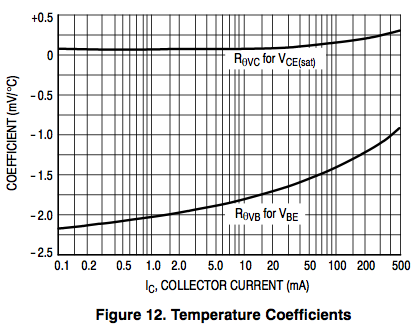
The bottom curve, RθVB for VBE, is essentially the same thing as what I described as \( \epsilon_T \); it’s given as a function of collector current, and is in absolute terms: mV/°C. The way you’d read the graph here is that at 15mA collector current, the tempco is -1.75mV/°C, so if the temperature at the npn junction went up by 10°C, you would expect the VBE drop to decrease by about 17.5mV.
There are temperature coefficients for lots of things in electronics. Op-amp datasheets will almost always give you the typical temperature coefficient for offset voltage: in the MCP6022, for example, it’s ±3.5μV/°C. Voltage references are another component: the LM4041 has a spec of no more than ±100ppm/°C, whereas the TL431 doesn’t give a tempco directly, just an allowed voltage deviation over the rated temperature range. Resistors will tell you the temperature coefficient of resistance; Yageo’s garden variety thick-film chip resistors have a tempco of ±100ppm/°C for values in the 10Ω - 10MΩ range, and ±200ppm/°C for the low- and high-value resistors. That’s pretty typical, and what you need to keep in perspective is that over a 50°C range, for instance, ±100ppm/°C will turn into a ±5000ppm = ±0.5% change, which is in addition to the ±1% base tolerance. So those ±1% resistors are really only ±1% if you treat them nicely and keep them at a constant temperature.
Temperature coefficients of electronic components usually fall into two categories.
The first category is when the temperature coefficient is centered around some known number. An example is the base-emitter voltage tempco of the 2N2222. We’re stuck with it, and if it matters to us, we have to care about it, and design our circuit to handle that behavior. Another is the resistance of copper wire, with a tempco of approximately 3930ppm/°C.
The other category occurs when the temperature coefficient is centered around zero, as in the LM4041 or in resistors. In this case, someone has done the work to use materials in a clever manner (e.g. manganin for resistors) or has designed an integrated circuit in such a way to cancel out the temperature coefficient as much as reasonably possible. So when you see ±100ppm/°C, it means the manufacturer has tried to produce a zero tempco, but some parts might be a little below zero or a little above zero, and if they hadn’t been clever, the tempco might be nonzero on average, and much higher.
Quartz crystals are particularly interesting in this respect. The temperature coefficient of the resonant frequency depends on the alignment of the crystal surfaces with the crystal lattice. Scientists and engineers have known this, and as a result, many of the quartz crystals used in electronic oscillators are of the AT cut variety, where the tempco is near zero around room temperature. The 32.768kHz crystals used for timekeeping are XY cut, with a tempco also around zero at room temperature. In these cases, there are still variations with temperature, they are just minimized around zero, and because this variation is predictable, the tempco is given as a parabolic temperature coefficient, in ppm/°C2, so the XY-cut tempco yields a frequency vs. temperature curve that looks like
$$ f = f_0 \left(1 + b(T-T_0)^2\right)$$
In an XY-cut timing crystal like the Epson FC1610AN, f0 = 32.768kHz, T0 = 25°C, and b = -0.04ppm/°C2.
The Wah-wah-wah-wah-wonder of Operational Amplifiers
And I wonder,
I wah-wah-wah-wah-wonder,
why,
why why why why why
she ran awayAnd I wonder,
where she will stay,
my little runaway
a-run-run-run-run-runaway— Del Shannon, Runaway
One of my electronics classes in college was an analog electronics lab. We studied all sorts of stuff you could do with bipolar transistors. In one of the labs we had to design an op-amp out of discrete transistors. In practice, you would never do this, because there’s no way you could come close to the performance of even the lousy 741 op-amp. The point was for us to learn something about how commercial op-amps work in practice, and to see that we could make it work even if we were stuck with discrete transistors.
Here’s the circuit equivalent from the LM741 opamp, the one we like to hate:
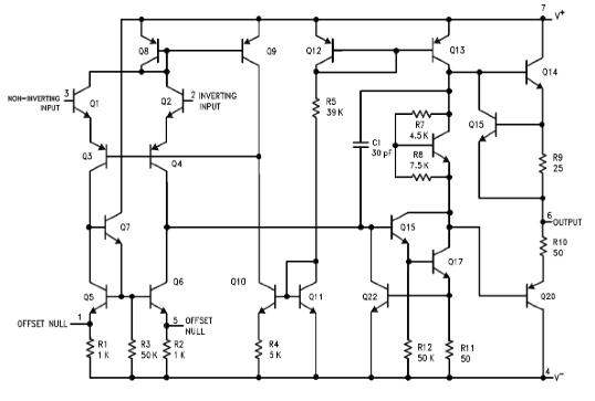
Doesn’t it look a lot like hieroglyphics?
To understand how an op-amp works, it helps to ignore the details and focus on the big picture. Here I’ve annotated the circuit diagram:
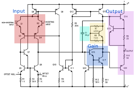
The input stage is made up of a differential pair of NPN and PNP transistors Q1-Q4; through the magic of transistor circuits, the difference in voltage between the inputs is turned into a current signal proportional to that voltage difference, and sent into the single-ended Darlington amplifier made up of Q15 and Q17. Resistors R7, R8, and the unlabeled transistor (Q16?) form a level-shifting circuit; C1 is the internal compensation capacitor that feeds back into the base of Q15; and transistors Q14 and Q20 form a push-pull output stage, with Q15 (the second Q15? Come on, National/TI, proofread your datasheets!) acting as a current limit. The rest of the circuitry is used to setup bias currents and act as an active load for the input stage.
The level-shifting circuit is kind of interesting, and you have to understand something about push-pull output stages to appreciate it.
Let’s say you have this circuit:
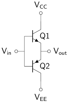
When the output stage formed by Q1 and Q2 is sourcing current, Q1 carries current and Vout is one VBE drop below Vin.
When the output stage formed by Q1 and Q2 is sinking current, Q2 carries current and Vout is one VBE drop above Vin.
This voltage shift, which depends on the direction of output current, is called crossover distortion. Right around zero current, the output voltage has to shift up or down by two VBE drops, or somewhere in the 1.2-1.5V range.
In the LM741 schematic, the two resistors R7 and R8 form a kind of adjustable voltage regulator across the unnamed transistor. The voltage across each resistor is roughly proportional to the resistance (current into the base terminal is small), so R8 sees a VBE drop and R7 sees about 4.5K/7.5K = 0.6VBE, for a total voltage drop of 1.6VBE or about 1.0-1.2V. This voltage shift pulls apart the transistors Q14 and Q20 so the crossover distortion is reduced by about 80%.
Our lab op-amp was much simpler than the LM741 schematic. We had some room to design our own circuit, but it had to be based on 2N3904 and 2N3906 NPN and PNP transistors. I seem to remember it had a limit of only 6 or 8 transistors, and it didn’t have to be as nicely-behaved as the 741 (I can’t believe I’m saying that; it’s like saying someone didn’t have to behave as nicely as Dick Cheney), but it had particular gain requirements up to a few megahertz, which can be challenging on a solderless breadboard.
I had got my circuit working, and was making measurements for my lab writeup, when I heard a POP on the other side of the lab, along with a few choice four-letter words, and maybe 30 seconds later that distinctive smell wafted through the room. You know, That Smell. Every electronics student should experience it at least once, but hopefully not very often. Yes, a component has overheated and lets the magic smoke out, sharing volatile organic compounds with the whole room. I looked over and saw the guy in question turn the power off, throw some transistors away, and replace them with new ones.
A few minutes after that, I heard another POP. I looked over and it was the same guy, and he replaced the transistors again. I knew the guy; he was a really smart student, but that day he was being stupid. (While writing this, I got curious and looked him up on Google. He’s now a successful partner in a business consulting firm. I guess EE just wasn’t his thing.) It dawned on me what the problem was. Here is what he used as an output stage in his circuit:

There were other components besides the ones shown here (something has to provide base current to the transistors; I think he had resistors from the diodes to VCC and VEE), but ignore that for a moment. The diodes essentially cancel out the VBE drops and remove all of the crossover distortion, making the output voltage identical to the input voltage. Very clever. His circuit did, in fact, work for a while, but then, after a minute or two, would go POP and die in a gasp of pungent smoke.
Now, there’s an issue here. Let’s look at one of the graphs we saw earlier, from the 2N2222A datasheet:
You will note that the VBE temperature coefficient is negative. That means that for a fixed amount of collector current, if the transistor heats up, the base-to-emitter voltage goes down. But what happens if you keep the voltage across the base-emitter junction fixed? Well, let’s say you were providing 0.7V and got 10mA. Now the transistor heats up by 1 degree C, so the base-emitter voltage goes down by about 1.8mV, so you only need 0.6982V to get 10mA. But you have 0.7V. And we said that every 18mV just about doubles the current. If you run the numbers, increasing base-emitter voltage by 1.8mV should increase the current by about 7%, to 10.7mA. So a 1 degree C rise in temperature increased collector current by 7%, from 10mA to 10.7mA.
Interesting.
When the transistor conducts more current, it dissipates power and heats up more. So maybe this causes it to rise another degree. And this, in turn, causes the required VBE drop to go down by 1.8mV, and increase the current another 7%, to about 11.5mA.
What we’ve got is a situation where more current causes the junction temperature to go up, which causes more current to flow. A positive feedback loop. This is called thermal runaway. And eventually, one of three things happens:
-
The extra power dissipation that heats up the transistor is balanced by environmental cooling (convection if the transistor is just sitting in air), and causes the junction temperature to stabilize.
-
The current increases enough that the tempco decreases in magnitude (at 100mA, the tempco is only about -1.4mV/°C), and this causes the current to stabilize. Though if you run the numbers, at 100mA, a 1.4mV decrease in required VBE causes about a 5.5% increase in current, to 105.5mA. This is still a pretty significant increase.
-
Something else happens (POP!) that disrupts the feedback loop.
So as long as the guy’s output current draw was low, the transistors had a chance of surviving. But as soon as there was enough current, the VBE voltage dropped enough to cause both output transistors to conduct, and thermal runaway took over, until the junction overheated and cracked the package, letting the magic smoke out and stopping the flow of current.
The 741 op-amp design has three design features to prevent thermal runaway:
- The level-shifting circuit to reduce crossover distortion doesn’t completely eliminate it, so both transistors are never on at the same time.
- There are emitter resistors in the output stage. These are called emitter ballast resistors, and they’re used to soften the knee of the transistor’s current vs. VBE curve at high currents.
- Emitter resistor R9 is connected to a transistor that eventually conducts and robs base current from the NPN output device, causing an active current limit. (I’m not sure why there isn’t one on the PNP side.)
Other Types of Thermal Runaway
There are plenty of other mechanisms for thermal runaway, so you should keep an eye on power dissipation in your circuit design, as well as the temperature coefficients. Three important ones in power electronics are the following:
-
The base-emitter voltage tempco is usually negative for bipolar power transistors. This means you can’t put them directly in parallel, or a similar kind of thing will happen: transistor A and B each carry 1A of current, but then B heats up a little more than A, so it tells A, “Hey, look, I can carry more current now, I’ll take 1.1A and you take 0.9A”, and then B heats up a little more, and it says, “Hey, I can carry more current now, I’ll take 1.2A and you take 0.8A” and eventually B takes almost all of the current. This is called current hogging. Even if you put resistors in series with the base, the negative collector-emitter voltage tempco for bipolar power transistors means that current hogging will occur. If you want to parallel bipolar transistors, you have to add emitter ballast resistors.
-
The on-resistance tempco is usually positive for MOSFETs, typically increasing by a factor of 1.5-2.5 between room temperature and the maximum operating temperature of the transistor. While this means you can parallel MOSFETs (if one heats up, its on-resistance will go up and that will reduce the current it conducts, compared to the other MOSFETs in parallel), it has a negative consequence for designs where the MOSFET load is a constant current, like a power converter or a motor controller. Let’s say the MOSFET carries 10A of current, so it heats up, and its on-resistance increases, so it heats up more, which makes its on-resistance increase further… until things either stabilize or you hear a loud POP. What you basically have to do is plan on the MOSFET resistance being its maximum value. If the thermal management of your system keeps the MOSFET junction temperature below its maximum limit, you’re OK, and in the end you’ll be conservative: instead of it getting to 150°C, it might only get to 125°C, so its on-resistance is a little less, which means the power dissipation is going to be less than you planned for.
-
The temperature coefficient of magnetic saturation is sometimes negative — I’m not 100% sure this is the case for all magnetic materials, but Murphy’s Law says it is — which means that when your inductors and transformers heat up, their inductance can drop. And if you’re using them in a switching power converter, this means their ripple current will increase, which means they will heat up more, until you get smoke and/or arcing. (I mentioned this in an earlier article.)
So don’t you wonder why, WHY WHY WHY WHY WHY they ran away — be vigilant and you’ll avoid thermal runaway.
Summary
We covered some miscellaneous circuit design topics today:
-
The base-emitter voltage in a bipolar transistor \( V_{BE} = \frac{nkT}{q} \ln \frac{I_C}{I_s} \) where n is the ideality factor, usually slightly greater than 1.0 for commercially-available transistors. This makes the current an exponential function of base-emitter voltage.
-
Linearization can help you understand the dynamic resistance of a component with a nonlinear V/I relationship, and solve circuit analysis problems more easily.
-
Many electronic components have parameters that change with temperature; the temperature coefficient tells how much they vary with temperature, and if you’re lucky it’s specified in the component datasheet.
-
Certain temperature coefficients can cause a positive feedback loop that causes components to heat up more when they get hotter, which is called thermal runaway.
Thanks for reading, and don’t let the magic smoke out!
© 2015 Jason M. Sachs, all rights reserved.


- Comments
- Write a Comment Select to add a comment
To post reply to a comment, click on the 'reply' button attached to each comment. To post a new comment (not a reply to a comment) check out the 'Write a Comment' tab at the top of the comments.
Please login (on the right) if you already have an account on this platform.
Otherwise, please use this form to register (free) an join one of the largest online community for Electrical/Embedded/DSP/FPGA/ML engineers:


