


Deeply embedded design example - Logic replacement
I have always believed that some of the low-cost, low-pin count, low-resource microprocessors would make an excellent choice for the replacement of discrete logic components. In these cases the deeply embedded microprocessor would become less of a general purpose computer and more of a logic replacement, providing a prescribed function with no connection to the outside world. In a world of bigger, faster and more expensive, it is a pleasant change of pace to embrace the smaller and cheaper, and build a slightly better mousetrap. The following is an account of such an undertaking.
Recently I was involved in a design review for a cost reduction project, where an older design was getting an update. The new design was a merging of two different designs, including some updated parts and some existing controls. The design includes six 10Amp H-bridge drivers and the associated control logic. Some of the early testing had shown some rather large current spikes and also some higher than desirable amounts of electromagnetic interference (EMI). A consultant who had been helping out on a similar design, mostly on EMI concerns, had suggested a few timing changes to the circuitry. As the talks continued, two different schemes involving changes to the timing were discussed. At this point, I had jumped in and suggested that we pull out all the control circuitry and replace it with a small microprocessor or a CPLD, allowing us some freedom to make changes in the timing schemes. My manager had referred to my suggestion as "a small joke", but I assured him I was serious.
A couple of days later I met with my manager and we talked a little more about the idea of handling the bridge control logic inside of a small microprocessor. After we are able to agree that it would in fact be possible (and also a good idea to do so), we quickly defined the desired level of control and the range of the different delays that we would need to consider.
Great, we have a plan and a direction. Before we jump into the work, let's take a moment and analyze the current circuit to determine present functionality and the actual delay times in order to better understand our starting point. The big picture view on the circuit is actually quite simple. Changes in the 'Direction' line require proper sequencing of the current source and the bridge drivers. On a change in direction, the presently selected drivers (opposite side, top and bottom MOSFETs) are disabled along with the programmable current source. Then a delay occurs before enabling the opposite set of MOSFETs, along with another delay prior to re-enabling the current source. It is the sequence of these actions and the time delays that will have effects on the operation and resulting EMI characteristics of our six H-bridges.
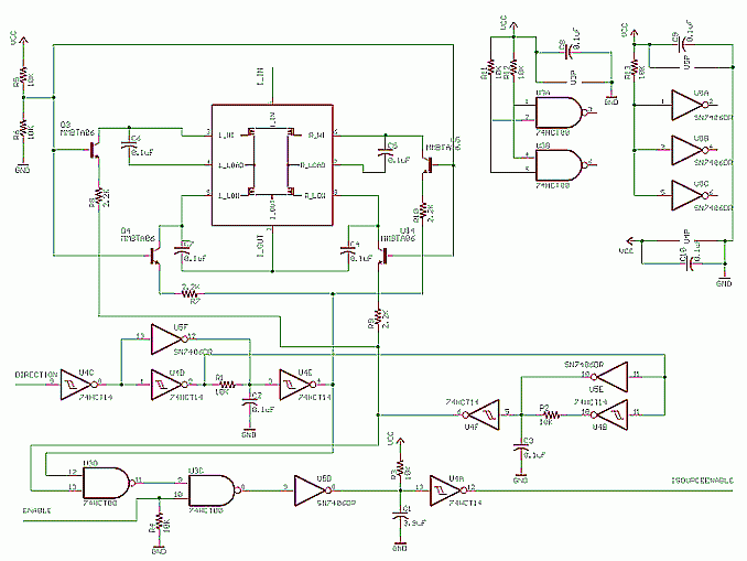
In the above schematic there are two different delay circuits (two copies using 10K and 0.1uF, plus one using 10 and 3.9uF). The direction control circuits each use two different inverters (an open collector type - SN7406 and a Schmitt trigger type - 74HTC14). Each of these inverters are use to control a different edge of the transitions, the Schmitt trigger controls the rising edge (enable), by applying a charging current through a series resistor into a timing capacitor (0.1uF) to cause a fixed delay, while the open collector inverter controls the falling edge (disable), by using a high current dump of the charge on the capacitor to effect a near zero delay turn off. The combination of the two inverter types is actually a clever approach. The Schmitt trigger device drives both high and low at ~4ma, while the Open Collector device provides no drive in high, but can sink ~40ma during the low state, providing controlled rise time and fast fall time.
The second delay circuit is used to control the programmable current source by temporarily disabling the current source during the direction changes. This stage uses a single Open Collector inverter to allow the timing cap to charge while the invert is high (through the 10K resistor to VCC) and then to discharge quickly through the device when its output is low. When the direction changes and one of the two delay circuits does the quick switch to disable, its output goes high (either U4E or U4F), while the other output is high (waiting to go low, or enable), the first NAND gate in the enable chain will see both of its input high, causing the output to go low. This causes the second NAND gate output to go high, in turn causing the invert output to go low, quickly discharging the 3.9uF capacitor, which causes the second inverter to go high, and thus disabling the current source. When the delayed H-bridge enable occurs, the first NAND sees a high and a low input causing its output to high, which in turn, causes the second NAND output to go low and the open collector inverter output to go high. This starts the charging (delay) cycle to begin, hold the current source disabled. Once the 3.9uF charges up to the high level for the Schmitt trigger input, its output toggles and the current source is re-enabled.
With the above circuits, the time delays are roughly as follows (component variations will effect results - all times are relative to detected change on the direction input):
- Driver turn off time - ~6us
- Current source disable - ~300us
- Opposite Drive turn on time - ~750us
- Current source re-enable - ~30ms
OK, it looks like we simply need to monitor the direction line and provide two lines to control the direction of current through our H-bridge and a single line to enable/disable the current source. This resource requirement seems to be a nice match to the PIC10F200 part. This is a six-pin, 8-bit microcontroller. It provides a 4MHz internal clock, yielding a 1us instruction cycle. With a whopping 256 instruction words (FLASH), 16 bytes of SRAM and a 8-bit timer/counter, it should be fully up to the task at hand.
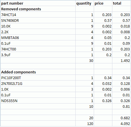
The task of generating an updated schematic was pretty simple, as there is only a handful of components per channel. Looking at the new schematic and changes in the Bill of Materials (BOM) below, the simplicity is quite clear. As the circuit is repeated six times within the board, the total part reduction was 120 components for a total savings of $4.092. The parts cost alone is only the start. Savings in terms of board real estate and assembly cost will add to the savings.
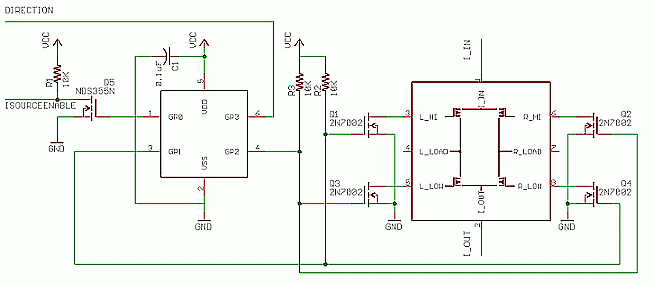
Before jumping into the code for our design, we should first outline the specifications. The bridge controller design is based on a PIC10F200T-E/OT, 6-pin microcontroller. The purpose of the PIC is replace the existing discrete logic circuits to control the direction of a power H-bridge, determined by the 'DIRECTION' input and to control the 'ISOURCEENABLE' line (wire 'AND' to a global current source enable line).
Upon startup, the PIC will configure the timer and watchdog, and then sample the 'DIRECTION' line to determine the starting state for the H-bridge. This starting state will be used to pre-condition debounce logic that will be used to assist in the rejection of spurious noise on the 'DIRECTION' input. The PIC should then use the starting state to condition the H-bridge with the proper starting direction.
In the debounce loop, the PIC should repeated sample the state of the 'DIRECTION' input, waiting for eight consecutive reading of the same level (while servicing the watchdog timer). When a change is detected, the PIC should first disable the current source, wait 1 ms, turn off all bridge drivers, wait 100us then enable the desired bridge drivers, then wait 100us before it re-enable the current source. After this process the PIC should revert to sampling the 'DIRECTION' line.
The PIC is configured will be configured to use the following pin assignments:
|
Pin # |
Name |
Direction |
Function - Description |
|
1 |
GP0 |
Output |
Current controller enable (Wired ‘AND’ to global enable) |
|
2 |
Vss |
Ground |
|
|
3 |
GP1 |
Output |
Bridge Left-High/ Right-Low enable |
|
4 |
GP2 |
Output |
Bridge Right-High/ Left-Low enable |
|
5 |
Vdd |
Vcc |
|
|
6 |
GP3 |
Input |
Hot/Cold input |
Furthermore, the PIC firmware will be designed to configure the following resources to following states/conditions:
- Internal 4MHz oscillator.
- No Mclr function (GP3 enabled).
- Watchdog timer enabled as a 'run away' protection, no divider, ~16 ms.
- Weak pull-ups enabled, wakeup on pin changes disabled.
- Timer 0, Fosc (4MHz) / 4 / 16, or ~16us clock source (providing support for time delays).
OK, now we have everything we need to write a program for the necessary control functions. The code is broken up into two modules, the first being the actual code (PWMcontrol.ASM) and the second the necessary bit and byte defines for the various ports and registers (PWMcontrol.INC). The source code was written in assembly in order to focus on the most efficient control of the PIC resources and to fully expose the time delays of the various loops and such. Here is the final listing of the assembly language in support of our design.
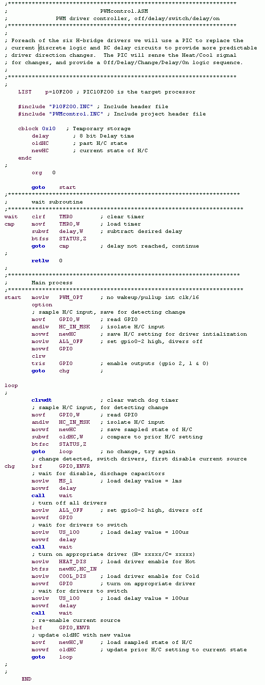
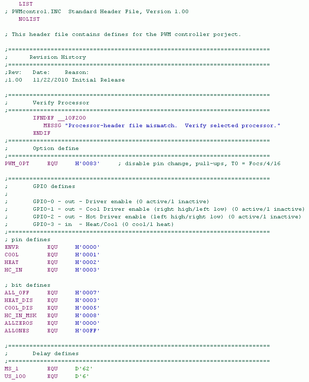
The PWMcontrol.INC file, contains the necessary bit and byte defines for the various ports and registers within the PIC10F200 and other defines targeted to our implementation.
Once everything was assembled and tested, the final tally of resources used within the PIC10F200 is as follows:
- 62 of 256 FLASH words (24%)
- 4 of 16 SRAM bytes (25%)
- 1 of 1 8-bit timers (100%)
- 4 of 4 I/O pins (100%)
The above figures show that there is still run for changes, should any be needed in the future. We had chosen this approach to provide flexibility for controllable timing changes. In the test and evaluations that followed this design, we were able to vary the delays, change the on/off sequencing and precisely tune the performance of the overall design in order to meet all the objectives that we had established, i.e. maximize performance (efficiency) while minimizing the EMI effects. AS of this writing the overall design is continuing to move forward, through reliability and environmental testing, heading towards a release as an update to an existing product.
Once again, thank you for following along. Happy embedding!
Gene


- Comments
- Write a Comment Select to add a comment
To post reply to a comment, click on the 'reply' button attached to each comment. To post a new comment (not a reply to a comment) check out the 'Write a Comment' tab at the top of the comments.
Please login (on the right) if you already have an account on this platform.
Otherwise, please use this form to register (free) an join one of the largest online community for Electrical/Embedded/DSP/FPGA/ML engineers:


